
WEMOS D1 MINI ESP32
WEMOS D1 MINI ESP32 is a development board based on the ESP32 microcontroller using XTENSA architecture.
This board features a maximum CPU frequency of 240 MHz and 4MB flash memory.
About WEMOS D1 MINI ESP32
The WEMOS D1 mini ESP32 squeezes Espressif’s dual-core ESP32-WROOM-32 module into the familiar 34 × 25 mm D1-mini footprint-so it drops straight into the huge ecosystem of D1-mini shields. Despite its tiny size it brings full-featured Wi-Fi 802.11 b/g/n and Bluetooth 4.2 (BLE + BR/EDR) connectivity to your IoT projects. 📡
A reliable CH340C USB-to-UART interface (auto-reset capable) lets you plug in via Micro-USB, flash code, and get serial logs with zero extra hardware. 🔌
Power is flexible: feed the board from
5 V on USB/VIN or directly from the regulated 3V3 pin. An on-board LDO and protective circuitry keep the ESP32 happy. ⚡️The board sports a tiny PCB antenna for solid RF performance, plus RST and BOOT (IO0) push-buttons to simplify firmware flashing and recovery. 🚀
All GPIOs support PWM, many provide ADC, DAC, I²C, SPI, UART, and ten pads double as capacitive-touch sensors. Stack it beneath sensor, relay, or display shields and you’ve got a compact yet powerful connected gadget in minutes. ⚙️
Where to Buy WEMOS D1 MINI ESP32

Starting from
6$ per unit


Prices are subject to change. We earn from qualifying purchases as an Amazon Associate.
Technical Specifications
Complete technical specification details for WEMOS D1 MINI ESP32
Quick Setup
Copy-paste configs for WEMOS D1 MINI ESP32 - auto‑generated from this board's exact hardware specs.
In Arduino IDE 2 select D1 Mini32 from the esp32 by Espressif package. In PlatformIO use board = esp32dev. ESP32 · 240 MHz · 4MB · DIO.
In Arduino IDE 2, open Boards Manager, search "esp32" by Espressif and install it. Then go to Tools → Board and select "D1 Mini32" for the WEMOS D1 MINI ESP32.
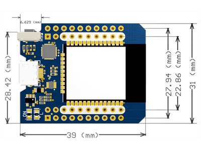
WEMOS D1 MINI ESP32 Board Dimensions
Physical measurements for WEMOS D1 MINI ESP32
WEMOS D1 MINI ESP32 Pinout Diagram
Complete pin reference for WEMOS D1 MINI ESP32
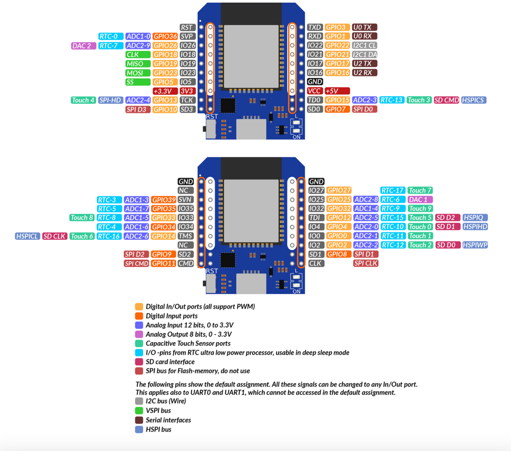
The WEMOS D1 mini ESP32 pinout exposes 26 ESP32 GPIOs on the familiar D label headers-making it shield-compatible while retaining the ESP32’s rich peripherals.
Power rails include 5 V/VIN (USB or external), a regulated 3V3 output, and multiple GND pins. Current draw is typically 80 mA active but can drop to <10 µA in deep-sleep.
Default serial lines U0_TX (GPIO1) and U0_RX (GPIO3) connect to the CH340C for programming and logging. Need another UART? Use U2_TX (GPIO17) and U2_RX (GPIO16).
I²C defaults to SDA (GPIO21) and SCL (GPIO22)-changeable in software-and breaks out on the D2/D1 shield pins.
SPI: the primary VSPI bus maps to MOSI GPIO23, MISO GPIO19, SCK GPIO18, and CS GPIO5. An alternate HSPI bus lives on GPIO12–15 when a second SPI device is needed.
Analog: Eight ADC1 channels on GPIO32–GPIO39 remain usable while Wi-Fi is active. Extra ADC2 channels (e.g., GPIO0, 2, 4, 12–15, 25–27) share hardware with Wi-Fi. Dual 8-bit DAC outputs are on GPIO25 and GPIO26.
Capacitive-touch sensing is available on GPIO0, 2, 4, 12–15, 27, 32, 33, perfect for touch-buttons or gesture pads.
Every GPIO can generate PWM up to 40 kHz for LEDs, motors, or buzzers. Watch the boot-strap pins-GPIO0, GPIO2, and GPIO15-which must be at the correct logic level (usually HIGH) at reset to boot normally.
With breadboard-friendly headers, shield compatibility, and the full might of an ESP32 module, the WEMOS D1 mini ESP32 pinout is your compact gateway to advanced connected projects.
Safe Pins to Use
These pins are safe for general GPIO usage without boot or system conflicts.
Pins to Avoid or Use with Caution
Reserved for critical functions. Misuse may cause boot failures, programming issues, or system conflicts.
| Pin | Label | Why Avoid | Type |
|---|---|---|---|
| IO14 | MTMS (GPIO14) | Used for JTAG debugging (TMS); driving it as GPIO may interfere with JTAG or produce spurious signals at boot. | 🪛 Other |
| IO12 | MTDI (GPIO12) | Keep LOW during boot (internal PD); pulling HIGH at reset selects 1.8V flash mode, causing flash brownout if 3.3V flash is used. | 🛠️ Strapping |
| IO13 | MTCK (GPIO13) | Used for JTAG debugging (TCK); avoid using as GPIO if JTAG is needed. | 🪛 Other |
| IO15 | MTDO (GPIO15) | Keep HIGH during boot (internal PU); if LOW on reset, bootloader log is silenced and boot mode may change. | 🛠️ Strapping |
| IO4 | GPIO4 | Sampled at reset for boot config; should not be driven at boot (affects boot mode timing). | 🛠️ Strapping |
Useful Links
Datasheets and resources for WEMOS D1 MINI ESP32
WEMOS D1 MINI ESP32 Custom Pin Mapping
Pin configuration and GPIO mapping for WEMOS D1 MINI ESP32
| Pin | Function | ESP Pin | I/O Type | Description |
|---|---|---|---|---|
| 1 | LED_BUILTIN | GPIO2 | output | On-board blue LED (active-LOW) |
| 2 | TXD | GPIO3 | output | UART0 Transmit (U0_TX) |
| 3 | RXD | GPIO1 | input | UART0 Receive (U0_RX) |
| 4 | SDA | GPIO21 | bidirectional | I²C Data Line |
| 5 | SCL | GPIO22 | bidirectional | I²C Clock Line |
| 6 | SS | GPIO5 | bidirectional | VSPI Chip-Select |
| 7 | MOSI | GPIO23 | bidirectional | VSPI Master-Out Slave-In |
| 8 | MISO | GPIO19 | bidirectional | VSPI Master-In Slave-Out |
| 9 | SCK | GPIO18 | bidirectional | VSPI Clock |
| 10 | A0 | GPIO36 | input | ADC1 Channel 0 |
| 11 | A3 | GPIO39 | input | ADC1 Channel 3 |
| 12 | A4 | GPIO32 | input | ADC1 Channel 4 / Touch 9 |
| 13 | A5 | GPIO33 | input | ADC1 Channel 5 / Touch 8 |
| 14 | DAC1 | GPIO25 | output | 8-bit Digital-to-Analog Converter 1 |
| 15 | DAC2 | GPIO26 | output | 8-bit Digital-to-Analog Converter 2 |
| 16 | IO27 | GPIO27 | bidirectional | Touch 7 / RTC-17 |
| 17 | IO14 | GPIO14 | bidirectional | HSPI SCK / Touch 6 |
| 18 | IO12 | GPIO12 | bidirectional | HSPI MISO / Touch 5 |
| 19 | IO13 | GPIO13 | bidirectional | HSPI MOSI / Touch 4 |
| 20 | IO15 | GPIO15 | bidirectional | Boot-strap Pin / Touch 3 |
| 21 | IO4 | GPIO4 | bidirectional | Touch 0 / ADC2 Channel 0 |
| 22 | RX2 | GPIO16 | bidirectional | UART2 Receive |
| 23 | TX2 | GPIO17 | bidirectional | UART2 Transmit |
| 24 | BOOT_IO0 | GPIO0 | bidirectional | Boot-mode Select / Touch 1 (keep HIGH to boot) |
| 25 | A6 | GPIO34 | input | ADC1 Channel 6 (input-only) |
| 26 | A7 | GPIO35 | input | ADC1 Channel 7 (input-only) |
Pin Mappings
Complete pinout and GPIO mapping for WEMOS D1 MINI ESP32
| Pin | Analog | Touch | PWM | Other |
|---|---|---|---|---|
| 1 | TXD | |||
| 2 | LED_BUILTIN | |||
| 3 | RXD | |||
| 5 | ||||
| 16 | ||||
| 17 | ||||
| 18 | ||||
| 19 | ||||
| 21 | ||||
| 22 | ||||
| 23 | ||||
| 26 | ||||
| 35 | _VBAT |
Default Tools & Configuration
Build and upload settings for WEMOS D1 MINI ESP32
| Setting | Value |
|---|---|
| Bootloader tool | esptool_py |
| Uploader tool | esptool_py |
| Network uploader tool | esp_ota |
| Bootloader address | 0x1000 |
| Flash mode | dio |
| Boot mode | dio |
| Maximum upload size | 1280 KB (1310720 bytes) |
| Maximum data size | 320 KB (327680 bytes) |
The WEMOS D1 MINI ESP32 uses esptool_py for uploads , esp_ota for OTA updates, and esptool_py bootloader at 0x1000.
Flash mode: dio | Boot mode: dio
Max sketch size: 1280 KB | Max data size: 320 KB
Similar Boards
Other development boards with ESP32 microcontroller

LOLIN S2 PICO
LOLIN S2 PICO development board is based on esp32s2 microcontroller and uses xtensa architecture.

LOLIN C3 Mini
LOLIN C3 Mini development board is based on esp32c3 microcontroller and uses riscv32 architecture.

WEMOS LOLIN32
WEMOS LOLIN32 development board is based on esp32 microcontroller and uses xtensa architecture.