
ESP32-WROOM
ESP32-WROOM is a development board based on the ESP32 microcontroller using XTENSA architecture.
This board features a maximum CPU frequency of 240 MHz and 4MB flash memory.
About ESP32-WROOM
The ESP32-WROOM-32 is a versatile and powerful Wi-Fi + Bluetooth® + Bluetooth LE module, designed to support a wide range of applications. It is equally suitable for low-power sensor networks as well as high-demand tasks like voice encoding, music streaming, and MP3 decoding.
At the heart of the module is the ESP32-D0WDQ6 chip, engineered for scalability and adaptability. This chip features two CPU cores that can be independently controlled, with an adjustable clock frequency ranging from 80 MHz to 240 MHz. Additionally, it includes a low-power coprocessor, which is ideal for handling tasks that require minimal computing power-such as peripheral monitoring-while conserving energy.
The ESP32 integrates a rich set of peripherals, including capacitive touch sensors, an SD card interface, Ethernet, high-speed SPI, UART, I2S, and I2C. Its combination of power, flexibility, and connectivity makes the ESP32-WROOM-32 a perfect choice for a broad spectrum of IoT and embedded applications.
Technical Specifications
Complete technical specification details for ESP32-WROOM
Quick Setup
Copy-paste configs for ESP32-WROOM - auto‑generated from this board's exact hardware specs.
In Arduino IDE 2 select Esp32 Wroom Da from the esp32 by Espressif package. In PlatformIO use board = esp32dev. ESP32 · 240 MHz · 4MB · DIO.
In Arduino IDE 2, open Boards Manager, search "esp32" by Espressif and install it. Then go to Tools → Board and select "Esp32 Wroom Da" for the ESP32-WROOM.
ESP32-WROOM Pinout Diagram
Complete pin reference for ESP32-WROOM
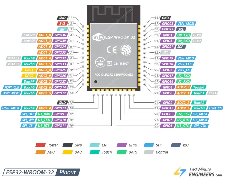
The ESP32-WROOM pinout is designed to offer developers a highly versatile and feature-packed layout for a variety of IoT and embedded applications. The ESP32 WROOM includes essential power pins such as 5V, 3.3V, and GND, ensuring stable power delivery for external components. Key communication protocols are well-supported, with pins for UART (RXD0, TXD0), SPI (MISO, MOSI, SCK, and SS), and I2C (SDA and SCL) to interface with a wide range of peripherals.
The ESP32 WROOM Devkit also supports multiple ADC pins (IO34, IO35, IO36, etc.), making it ideal for projects that require analog input, such as reading sensor data. Additionally, specialized pins such as DAC (IO25, IO26) and Touch Pins enhance its usability in advanced applications. The inclusion of RTC GPIOs further adds low-power features, allowing developers to take full advantage of the ESP32-WROOM pinout for efficient power management.
Safe Pins to Use
These pins are safe for general GPIO usage without boot or system conflicts.
Pins to Avoid or Use with Caution
Reserved for critical functions. Misuse may cause boot failures, programming issues, or system conflicts.
| Pin | Label | Why Avoid | Type |
|---|---|---|---|
| IO34 | GPIO34 | Cannot be used as output (no drive capability); only suitable for analog/digital input. | 🪛 Other |
| IO35 | GPIO35 | Cannot be used as output; only suitable for input. | 🪛 Other |
| IO14 | MTMS (GPIO14) | Used for JTAG debugging (TMS); driving it as GPIO may interfere with JTAG or produce spurious signals at boot. | 🪛 Other |
| IO12 | MTDI (GPIO12) | Keep LOW during boot (internal PD); pulling HIGH at reset selects 1.8V flash mode, causing flash brownout if 3.3V flash is used. | 🛠️ Strapping |
| IO13 | MTCK (GPIO13) | Used for JTAG debugging (TCK); avoid using as GPIO if JTAG is needed. | 🪛 Other |
| IO15 | MTDO (GPIO15) | Keep HIGH during boot (internal PU); if LOW on reset, bootloader log is silenced and boot mode may change. | 🛠️ Strapping |
| IO2 | GPIO2 | If driven HIGH on reset (while IO0 is LOW), selects an unsupported SDIO boot mode, causing boot failure. | 🛠️ Strapping |
| IO0 | GPIO0 | Must be HIGH during boot for normal startup; if held LOW on reset, forces flash programming mode. | 🛠️ Strapping |
| IO4 | GPIO4 | Sampled at reset for boot config; should not be driven at boot (affects boot mode timing). | 🛠️ Strapping |
| IO16 | GPIO16 | Connected to internal PSRAM on PSRAM-enabled modules; not usable as GPIO on those modules. | ⚡ Flash |
| IO17 | GPIO17 | Connected to internal PSRAM on PSRAM-enabled modules; not usable as GPIO on those modules. | ⚡ Flash |
| IO5 | GPIO5 | Must be HIGH during boot; if pulled LOW at reset, alters SDIO slave timing and may prevent normal boot. | 🛠️ Strapping |
Useful Links
Datasheets and resources for ESP32-WROOM
ESP32-WROOM Custom Pin Mapping
Pin configuration and GPIO mapping for ESP32-WROOM
| Pin | Function | ESP Pin | I/O Type | Description |
|---|---|---|---|---|
| 1 | SENSOR_VP | GPIO36 | input | ADC1_CH0, RTC_GPIO0 |
| 2 | SENSOR_VN | GPIO39 | input | ADC1_CH3, RTC_GPIO3 |
| 3 | IO34 | GPIO34 | input | ADC1_CH6, RTC_GPIO4 |
| 4 | IO35 | GPIO35 | input | ADC1_CH7, RTC_GPIO5 |
| 5 | IO32 | GPIO32 | bidirectional | XTAL_32K_P (32.768 kHz crystal oscillator input), ADC1_CH4, TOUCH9, RTC_GPIO9 |
| 6 | IO33 | GPIO33 | bidirectional | XTAL_32K_N (32.768 kHz crystal oscillator output), ADC1_CH5, TOUCH8, RTC_GPIO8 |
| 7 | IO25 | GPIO25 | bidirectional | DAC_1, ADC2_CH8, RTC_GPIO6, EMAC_RXD0 |
| 8 | IO26 | GPIO26 | bidirectional | DAC_2, ADC2_CH9, RTC_GPIO7, EMAC_RXD1 |
| 9 | IO27 | GPIO27 | bidirectional | ADC2_CH7, TOUCH7, RTC_GPIO17, EMAC_RX_DV |
| 10 | IO14 | GPIO14 | bidirectional | ADC2_CH6, TOUCH6, RTC_GPIO16, MTMS, HSPICLK, HS2_CLK, SD_CLK, EMAC_TXD2 |
| 11 | IO12 | GPIO12 | bidirectional | ADC2_CH5, TOUCH5, RTC_GPIO15, MTDI, HSPIQ, HS2_DATA2, SD_DATA2, EMAC_TXD3 |
| 12 | GND | N/A | power ground | Ground connection |
| 13 | IO13 | GPIO13 | bidirectional | ADC2_CH4, TOUCH4, RTC_GPIO14, MTCK, HSPID, HS2_DATA3, SD_DATA3, EMAC_RX_ER |
| 14 | SHD/SD2 | GPIO9 | bidirectional | SD_DATA2, SPIHD, HS1_DATA2, U1RXD |
| 15 | SWP/SD3 | GPIO10 | bidirectional | SD_DATA3, SPIWP, HS1_DATA3, U1TXD |
| 16 | SCS/CMD | GPIO11 | bidirectional | SD_CMD, SPICS0, HS1_CMD, U1RTS |
| 17 | SCK/CLK | GPIO6 | bidirectional | SD_CLK, SPICLK, HS1_CLK, U1CTS |
| 18 | SDO/SD0 | GPIO7 | bidirectional | SD_DATA0, SPIQ, HS1_DATA0, U2RTS |
| 19 | SDI/SD1 | GPIO8 | bidirectional | SD_DATA1, SPID, HS1_DATA1, U2CTS |
| 20 | IO15 | GPIO15 | bidirectional | ADC2_CH3, TOUCH3, MTDO, HSPICS0, RTC_GPIO13, HS2_CMD, SD_CMD, EMAC_RXD3 |
| 21 | IO2 | GPIO2 | bidirectional | ADC2_CH2, TOUCH2, RTC_GPIO12, HSPIWP, HS2_DATA0, SD_DATA0 |
| 22 | IO0 | GPIO0 | bidirectional | ADC2_CH1, TOUCH1, RTC_GPIO11, CLK_OUT1, EMAC_TX_CLK |
| 23 | IO4 | GPIO4 | bidirectional | ADC2_CH0, TOUCH0, RTC_GPIO10, HSPIHD, HS2_DATA1, SD_DATA1, EMAC_TX_ER |
| 24 | IO16 | GPIO16 | bidirectional | HS1_DATA4, U2RXD, EMAC_CLK_OUT |
| 25 | IO17 | GPIO17 | bidirectional | HS1_DATA5, U2TXD, EMAC_CLK_OUT_180 |
| 26 | IO5 | GPIO5 | bidirectional | VSPICS0, HS1_DATA6, EMAC_RX_CLK |
| 27 | IO18 | GPIO18 | bidirectional | VSPICLK, HS1_DATA7 |
| 28 | IO19 | GPIO19 | bidirectional | VSPIQ, U0CTS, EMAC_TXD0 |
| 29 | NC | N/A | not connected | No connection |
| 30 | IO21 | GPIO21 | bidirectional | VSPIHD, EMAC_TX_EN |
| 31 | RXD0 | GPIO3 | bidirectional | U0RXD, CLK_OUT2 |
| 32 | TXD0 | GPIO1 | bidirectional | U0TXD, CLK_OUT3, EMAC_RXD2 |
| 33 | IO22 | GPIO22 | bidirectional | VSPIWP, U0RTS, EMAC_TXD1 |
| 34 | IO23 | GPIO23 | bidirectional | VSPID, HS1_STROBE |
| 35 | GND | N/A | power ground | Ground connection |
Pin Mappings
Complete pinout and GPIO mapping for ESP32-WROOM
| Pin | Analog | Touch | PWM | Other |
|---|---|---|---|---|
| 0 | A11 | T1 | ||
| 1 | PWM | TX | ||
| 2 | A12 | T2 | PWM | ANT1 |
| 3 | PWM | RX | ||
| 4 | A10 | T0 | PWM | |
| 5 | PWM | SS | ||
| 12 | A15 | T5 | PWM | |
| 13 | A14 | T4 | PWM | |
| 14 | A16 | T6 | PWM | |
| 15 | A13 | T3 | PWM | |
| 18 | PWM | SCK | ||
| 19 | PWM | MISO | ||
| 21 | PWM | SDA | ||
| 22 | PWM | SCL | ||
| 23 | PWM | MOSI | ||
| 25 | A18 | PWM | DAC1 ANT2 | |
| 26 | A19 | PWM | DAC2 | |
| 27 | A17 | T7 | PWM | |
| 32 | A4 | T9 | PWM | |
| 33 | A5 | T8 | PWM | |
| 34 | A6 | |||
| 35 | A7 | |||
| 36 | A0 | |||
| 39 | A3 |
Default Tools & Configuration
Build and upload settings for ESP32-WROOM
| Setting | Value |
|---|---|
| Bootloader tool | esptool_py |
| Uploader tool | esptool_py |
| Network uploader tool | esp_ota |
| Bootloader address | 0x1000 |
| Flash mode | dio |
| Boot mode | dio |
| Maximum upload size | 1280 KB (1310720 bytes) |
| Maximum data size | 320 KB (327680 bytes) |
The ESP32-WROOM uses esptool_py for uploads , esp_ota for OTA updates, and esptool_py bootloader at 0x1000.
Flash mode: dio | Boot mode: dio
Max sketch size: 1280 KB | Max data size: 320 KB
Similar Boards
Other development boards with ESP32 microcontroller

MH ET LIVE ESP32DevKIT
MH ET LIVE ESP32DevKIT development board is based on esp32 microcontroller and uses xtensa architecture.

Espressif ESP32-LyraT-Mini
Espressif ESP32-LyraT-Mini development board is based on esp32 microcontroller and uses xtensa architecture.

Frog Board ESP32
Frog Board ESP32 development board is based on esp32 microcontroller and uses xtensa architecture.