
ESP32 C3 Zero
ESP32 C3 Zero is a development board based on the ESP32C3 microcontroller using RISCV32 architecture.
This board features a maximum CPU frequency of 160 MHz and 4MB flash memory.
About ESP32 C3 Zero
The ESP32-C3-Zero is a compact development board featuring the Espressif ESP32-C3FN4 chip. It offers 2.4GHz Wi-Fi (802.11 b/g/n) and Bluetooth 5 (LE), making it ideal for IoT projects needing reliable wireless connectivity. 📶
Its small form factor makes it easy to integrate into space-constrained projects, and the onboard ceramic antenna ensures stable wireless performance without requiring an external antenna.
For ease of use, it includes a BOOT button and a RESET button, simplifying development and debugging. 🚀
With 15 GPIO pins and support for multiple interfaces (SPI, I2C, UART, I2S, ADC), the ESP32-C3-Zero is a flexible choice for your next embedded project! ⚙️
Where to Buy ESP32 C3 Zero

Starting from
$4.90 per unit


Prices are subject to change. We earn from qualifying purchases as an Amazon Associate.
Technical Specifications
Complete technical specification details for ESP32 C3 Zero
Quick Setup
Copy-paste configs for ESP32 C3 Zero - auto‑generated from this board's exact hardware specs.
In Arduino IDE 2 select Esp32c3 Dev from the esp32 by Espressif package. In PlatformIO use board = esp32-c3-devkitm-1. ESP32C3 · 160 MHz · 4MB · QIO · RISC-V.
In Arduino IDE 2, open Boards Manager, search "esp32" by Espressif and install it. Then go to Tools → Board and select "Esp32c3 Dev" for the ESP32 C3 Zero.
ESP32 C3 Zero Pinout Diagram
Complete pin reference for ESP32 C3 Zero
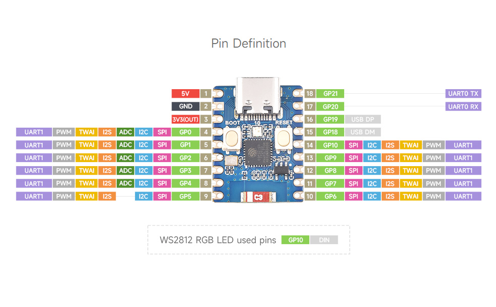
The ESP32-C3-Zero pinout is designed for maximum versatility in a compact size. Key power pins include 5V, 3.3V, and GND, ensuring stable power for various peripherals.
The board features multiple communication interfaces:
- UART: RX, TX
- I2C: SDA, SCL
- SPI: SCK, MISO, MOSI, SS
For analog input, it provides ADC pins suitable for reading sensor data or voltage levels.
Safe Pins to Use
These pins are safe for general GPIO usage without boot or system conflicts.
Pins to Avoid or Use with Caution
Reserved for critical functions. Misuse may cause boot failures, programming issues, or system conflicts.
| Pin | Label | Why Avoid | Type |
|---|---|---|---|
| IO2 | GPIO2 | Must be held high during boot (if low on reset, normal flash boot may fail) | 🛠️ Strapping |
| IO4 | MTMS | Used during boot; JTAG TMS for debugging; acts as Quad-SPI flash IO (hold data line) in internal-flash variants | 🔗 JTAG |
| IO5 | MTDI | Used during boot; JTAG TDI for debugging; acts as Quad-SPI flash IO (write-protect data line) in internal-flash variants | 🔗 JTAG |
| IO6 | MTCK | Used during boot; JTAG TCK for debugging; provides flash clock in internal-flash variants | 🔗 JTAG |
| IO7 | MTDO | Used during boot; JTAG TDO for debugging; acts as Quad-SPI flash IO (data line) in internal-flash variants | 🔗 JTAG |
| IO8 | GPIO8 | Must be held high during reset (if low, UART flashing/boot may not work) | 🛠️ Strapping |
| IO9 | GPIO9 | Controls boot mode on reset (HIGH for normal flash boot, LOW enters serial download mode) | 🛠️ Strapping |
| IO18 | USB_D- | By default connected to on-chip USB Serial/JTAG controller; to use as GPIO it must be reconfigured from its USB function | 🔌 USB |
| IO19 | USB_D+ | By default connected to on-chip USB Serial/JTAG controller; not available for GPIO use unless USB functionality is disabled or remapped | 🔌 USB |
| IO20 | U0RXD | Used as UART0 receive (console/bootloader); repurposing may disable serial programming and debug logs | 📡 UART |
| IO21 | U0TXD | Used as UART0 transmit (console/bootloader); repurposing may disable serial console output and printing | 📡 UART |
ESP32 C3 Zero Additional Information
More details about ESP32 C3 Zero

Useful Links
Datasheets and resources for ESP32 C3 Zero
ESP32 C3 Zero Custom Pin Mapping
Pin configuration and GPIO mapping for ESP32 C3 Zero
| Pin | Function | ESP Pin | I/O Type | Description |
|---|---|---|---|---|
| 1 | 5V | 5V | POWER INPUT | 5V power input for the board |
| 2 | GND | GND | POWER GROUND | Ground connection |
| 3 | 3V3 | 3.3V | POWER OUTPUT | 3.3V power output |
| 4 | IO0 | IO0 | BIDIRECTIONAL | GPIO, ADC |
| 5 | IO1 | IO1 | BIDIRECTIONAL | GPIO, ADC |
| 6 | IO2 | IO2 | BIDIRECTIONAL | GPIO, ADC |
| 7 | IO3 | IO3 | BIDIRECTIONAL | GPIO, ADC |
| 8 | IO4 | IO4 | BIDIRECTIONAL | GPIO, ADC |
| 9 | IO5 | IO5 | BIDIRECTIONAL | GPIO |
| 10 | IO6 | IO6 | BIDIRECTIONAL | GPIO |
| 11 | IO7 | IO7 | BIDIRECTIONAL | GPIO |
| 12 | IO8 | SDA | BIDIRECTIONAL | GPIO |
| 13 | IO9 | SCL | BIDIRECTIONAL | GPIO |
| 14 | IO10 | RX | BIDIRECTIONAL | GPIO, LED |
| 15 | IO18 | RX | BIDIRECTIONAL | USB DP |
| 16 | IO19 | RX | BIDIRECTIONAL | USB DM |
| 17 | IO20 | RX | BIDIRECTIONAL | GPIO, UART Receive (secondary) |
| 18 | IO21 | TX | BIDIRECTIONAL | GPIO, UART Transmit |
Pin Mappings
Complete pinout and GPIO mapping for ESP32 C3 Zero
| Pin | Analog | Touch | PWM | Other |
|---|---|---|---|---|
| 0 | IO0 | |||
| 1 | IO1 | |||
| 2 | IO2 | |||
| 3 | IO3 | |||
| 4 | SCK IO4 | |||
| 5 | MISO IO5 | |||
| 6 | MOSI IO6 | |||
| 7 | SS IO7 | |||
| 8 | LED_BUILTIN SDA IO8 | |||
| 9 | SCL IO9 | |||
| 20 | RX IO20 | |||
| 21 | TX IO21 |
Default Tools & Configuration
Build and upload settings for ESP32 C3 Zero
| Setting | Value |
|---|---|
| Bootloader tool | esptool_py |
| Uploader tool | esptool_py |
| Network uploader tool | esp_ota |
| Bootloader address | 0x0 |
| Flash mode | qio |
| Boot mode | qio |
| Maximum upload size | 1280 KB (1310720 bytes) |
| Maximum data size | 320 KB (327680 bytes) |
The ESP32 C3 Zero uses esptool_py for uploads , esp_ota for OTA updates, and esptool_py bootloader at 0x0.
Flash mode: qio | Boot mode: qio
Max sketch size: 1280 KB | Max data size: 320 KB
Similar Boards
Other development boards with ESP32C3 microcontroller

Deneyap Kart G
Deneyap Kart G development board is based on esp32c3 microcontroller and uses riscv32 architecture.

CYD ESP32-2424S012
CYD ESP32-2424S012 development board is based on esp32c3 microcontroller and uses xtensa architecture.

Espressif ESP32-C3-LCDKit
Espressif ESP32-C3-LCDKit development board is based on esp32c3 microcontroller and uses riscv architecture.