
ESP32S3 Walter Module
ESP32S3 Walter Module is a development board based on the ESP32S3 microcontroller using XTENSA architecture.
This board features a maximum CPU frequency of 240 MHz and 16MB flash memory.
About ESP32S3 Walter Module
Walter is a small, highly integrated IoT module built to tackle complex connectivity and processing needs. At its core is the ESP32-S3, a versatile system-on-chip (SoC) featuring a dual-core processor with hardware acceleration for machine learning, cryptography, and signal processing. It includes a range of peripherals, such as UART, SPI, I²C, and CAN, alongside built-in Wi-Fi b/g/n and Bluetooth 5, providing robust local networking and communication options.
What sets Walter apart is its inclusion of the Sequans GM02SP modem, offering LTE-M and NB-IoT 5G connectivity for low-power, wide-area communication, ideal for IoT applications. The modem also integrates a GNSS receiver, adding precise positioning capabilities for tasks like asset tracking, navigation, or geolocation.
Technical Specifications
Complete technical specification details for ESP32S3 Walter Module
Quick Setup
Copy-paste configs for ESP32S3 Walter Module - auto‑generated from this board's exact hardware specs.
In Arduino IDE 2 select Esp32s3 Dev from the esp32 by Espressif package. In PlatformIO use board = esp32-s3-devkitm-1. ESP32S3 · 240 MHz · 16MB · DIO.
In Arduino IDE 2, open Boards Manager, search "esp32" by Espressif and install it. Then go to Tools → Board and select "Esp32s3 Dev" for the ESP32S3 Walter Module.
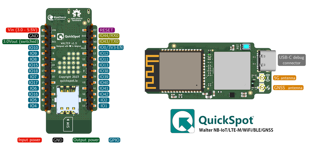
ESP32S3 Walter Module Pinout Diagram
Complete pin reference for ESP32S3 Walter Module
Safe Pins to Use
These pins are safe for general GPIO usage without boot or system conflicts.
Pins to Avoid or Use with Caution
Reserved for critical functions. Misuse may cause boot failures, programming issues, or system conflicts.
| Pin | Label | Why Avoid | Type |
|---|---|---|---|
| IO12 | FSPICLK | Drives the flash (and PSRAM) clock. This critical signal must be reserved for memory and not used as general GPIO. | ⚡ Flash |
| IO11 | FSPID | Used as a data line for flash (and in-package PSRAM). It should not be used as GPIO when the flash/PSRAM is in use. | ⚡ Flash |
| IO13 | FSPIQ | Used as a data line for flash/PSRAM transfers. Not available for other uses when flash/PSRAM is connected. | ⚡ Flash |
| IO38 | FSPIWP | On flash-equipped chips, this pin is tied to the flash’s WP# (or D3) line. It should be avoided for other use, as it’s needed for flash operations. | ⚡ Flash |
| IO39 | MTCK (GPIO39) | Default JTAG debugging TCK pin. If JTAG is needed, this pin must be free; it may also be used internally for PSRAM chip select on certain modules, so avoid repurposing it. | 🪛 Other |
| IO40 | MTDO (GPIO40) | Default JTAG TDO output for debugging. Using it as GPIO will interfere with JTAG debugging functionality. | 🪛 Other |
| IO41 | MTDI (GPIO41) | Default JTAG TDI input for debugging. Should be reserved for JTAG or left unused if JTAG is to remain available. | 🪛 Other |
| IO42 | MTMS (GPIO42) | Default JTAG TMS signal for debugging. Using this pin for other purposes will disable the JTAG interface (unless JTAG is rerouted to USB). | 🪛 Other |
| IO9 | FSPIHD | Connected to external flash (data/hold signal) on most modules. Not recommended for use as GPIO, since it must remain dedicated to flash communication. | ⚡ Flash |
| IO10 | FSPICS0 | Used to select the external flash chip. It is required for flash access and cannot be repurposed without losing flash connectivity | ⚡ Flash |
Useful Links
Datasheets and resources for ESP32S3 Walter Module
ESP32S3 Walter Module Custom Pin Mapping
Pin configuration and GPIO mapping for ESP32S3 Walter Module
| Pin | Function | ESP Pin | I/O Type | Description |
|---|---|---|---|---|
| 1 | RESET | EN | input | ESP32 reset with 10k pullup |
| 2 | IO44/RX0 | RXD0 | bidirectional | ESP32 UART0 Receive |
| 3 | IO43/TX0 | TXD0 | bidirectional | ESP32 UART0 Transmit |
| 4 | DFU/3V3 EN | IO0 | bidirectional | DFU when low on boot and 3V3 output enable |
| 5 | IO12 | IO12 | bidirectional | General purpose I/O |
| 6 | IO11 | IO11 | bidirectional | General purpose I/O |
| 7 | IO13 | IO13 | bidirectional | General purpose I/O |
| 8 | IO38 | IO38 | bidirectional | General purpose I/O |
| 9 | IO39 | IO39 | bidirectional | General purpose I/O |
| 10 | IO40 | IO40 | bidirectional | General purpose I/O |
| 11 | IO41 | IO41 | bidirectional | General purpose I/O |
| 12 | IO42 | IO42 | bidirectional | General purpose I/O |
| 13 | IO2 | IO2 | bidirectional | General purpose I/O |
| 14 | IO1 | IO1 | bidirectional | General purpose I/O |
| 15 | IO4 | IO4 | bidirectional | General purpose I/O |
| 16 | IO5 | IO5 | bidirectional | General purpose I/O |
| 17 | IO6 | IO6 | bidirectional | General purpose I/O |
| 18 | IO7 | IO7 | bidirectional | General purpose I/O |
| 19 | IO15 | IO15 | bidirectional | General purpose I/O |
| 20 | IO16 | IO16 | bidirectional | General purpose I/O |
| 21 | IO17 | IO17 | bidirectional | General purpose I/O |
| 22 | IO18 | IO18 | bidirectional | General purpose I/O |
| 23 | IO8 | IO8 | bidirectional | General purpose I/O |
| 24 | IO9 | IO9 | bidirectional | General purpose I/O |
| 25 | IO10 | IO10 | bidirectional | General purpose I/O |
| 26 | 3V3 OUT | N/A | power output | Switchable 3.3VDC output |
| 27 | GND | GND | power ground | GND connection |
| 28 | VIN | N/A | power input | DC Power input port |
Default Tools & Configuration
Build and upload settings for ESP32S3 Walter Module
| Setting | Value |
|---|---|
| Bootloader tool | esptool_py |
| Uploader tool | esptool_py |
| Network uploader tool | esp_ota |
| Bootloader address | 0x0 |
| Flash mode | dio |
| Boot mode | qio |
| PSRAM type | qspi |
The ESP32S3 Walter Module uses esptool_py for uploads , esp_ota for OTA updates, and esptool_py bootloader at 0x0.
Flash mode: dio | Boot mode: qio | PSRAM: qspi
Similar Boards
Other development boards with ESP32S3 microcontroller

Adafruit ESP32 Feather
Adafruit ESP32 Feather development board is based on esp32 microcontroller and uses xtensa architecture.

Adafruit Feather ESP32-S2 Reverse TFT
Adafruit Feather ESP32-S2 Reverse TFT development board is based on esp32s2 microcontroller and uses xtensa...

Adafruit Feather ESP32-S2 TFT
Adafruit Feather ESP32-S2 TFT development board is based on esp32s2 microcontroller and uses xtensa...