
TTGO T7 V1.3 Mini32
Compact ESP32 dev board with auto-reset and USB - ideal for space-saving Wi-Fi/BLE applications.

TTGO T7 V1.3 Mini32 Pinout
40 pins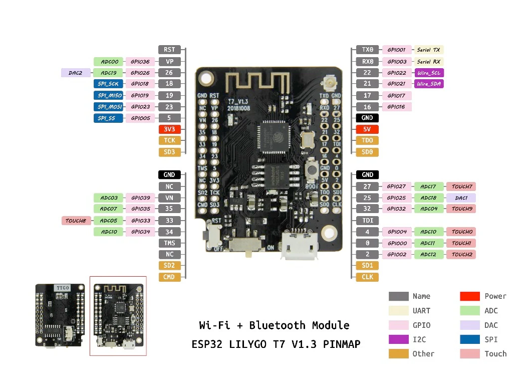
| Pin | GPIO | Labels | Status | Capabilities | Notes |
|---|---|---|---|---|---|
| 1 | - | RST | control | - | Reset (chip enable, active low) |
| 2 | 36 | VPGPIO36 | strapping | adc | ADC1_CH0, input only |
| 3 | 26 | 26GPIO26 | safe | adc · dac | DAC2, ADC2_CH9 |
| 4 | 18 | 18GPIO18 | safe | spi | VSPI SCK |
| 5 | 19 | 19GPIO19 | safe | spi | VSPI MISO |
| 6 | 23 | 23GPIO23 | safe | spi | VSPI MOSI |
| 7 | 5 | 5GPIO5 | strapping | spi | VSPI CS |
| 8 | - | 3V33.3V | power | - | 3.3V regulated output |
| 9 | 13 | TCKGPIO13 | strapping | - | JTAG TCK (MTCK) |
| 10 | 10 | SD3GPIO10 | strapping | - | Flash pin - do not use |
| 11 | - | GND | ground | - | Ground |
| 12 | - | NC | safe | - | Not connected |
| 13 | 39 | VNGPIO39 | strapping | adc | ADC1_CH3, input only |
| 14 | 35 | 35GPIO35 | strapping | adc | ADC1_CH7, input only |
| 15 | 33 | 33GPIO33 | safe | adc · touch | ADC1_CH5, Touch8 |
| 16 | 34 | 34GPIO34 | strapping | adc | ADC1_CH6, input only |
| 17 | 14 | TMSGPIO14 | strapping | - | JTAG TMS (MTMS) |
| 18 | - | NC | safe | - | Not connected |
| 19 | 9 | SD2GPIO9 | strapping | - | Flash pin - do not use |
| 20 | 11 | CMDGPIO11 | strapping | - | Flash pin - do not use |
| 21 | 1 | TX0GPIO1 | uart | uart | UART0 TX (USB serial) |
| 22 | 3 | RX0GPIO3 | uart | uart | UART0 RX (USB serial) |
| 23 | 22 | 22GPIO22LED_BUILTIN | safe | i2c | Default I2C SCL; onboard LED (LED_BUILTIN) |
| 24 | 21 | 21GPIO21 | safe | i2c | Default I2C SDA |
| 25 | 17 | 17GPIO17 | safe | - | General-purpose IO |
| 26 | 16 | 16GPIO16 | safe | - | General-purpose IO |
| 27 | - | GND | ground | - | Ground |
| 28 | - | 5V | power | - | 5V from USB, input to onboard regulator |
| 29 | 15 | TDOGPIO15 | strapping | - | JTAG TDO (MTDO) |
| 30 | 7 | SD0GPIO7 | strapping | - | Flash pin - do not use |
| 31 | - | GND | ground | - | Ground |
| 32 | 27 | 27GPIO27 | safe | adc · touch | ADC2_CH7, Touch7 |
| 33 | 25 | 25GPIO25 | safe | adc · dac | DAC1, ADC2_CH8 |
| 34 | 32 | 32GPIO32 | safe | adc · touch | ADC1_CH4, Touch9 |
| 35 | 12 | TDIGPIO12 | strapping | - | JTAG TDI (MTDI) |
| 36 | 4 | 4GPIO4 | safe | adc · touch | ADC2_CH0, Touch0 |
| 37 | 0 | 0GPIO0 | strapping | adc · touch | ADC2_CH1, Touch1, Boot button |
| 38 | 2 | 2GPIO2 | strapping | adc · touch | ADC2_CH2, Touch2 |
| 39 | 8 | SD1GPIO8 | strapping | - | Flash pin - do not use |
| 40 | 6 | CLKGPIO6 | strapping | - | Flash pin - do not use |
Start with these
13 pins with no boot or system involvementFreely assignable - no strapping, flash, USB or JTAG duties. Ideal first picks for buttons, sensors and LEDs.
Fine - with a little care
13 pins · 12 things to knowVPGPIO36 Input-only GPIO (no output); ADC1 channel 0, Hall sensor VP. Other
Cannot be used as output; only suitable for input (e.g., analog read).
5GPIO5 Bootstrapping pin; internal pull-up; VSPI CS0 (default SPI chip-select); acts as FSPIWP (flash write-protect) on internal-flash variants. Strapping
Must be HIGH during boot; if pulled LOW at reset, alters SDIO slave timing and may prevent normal boot.
TCKGPIO13 JTAG clock pin (TCK); also ADC2 channel 4 / Touch4 input. JTAG
Used for JTAG debugging (TCK); avoid using as GPIO if JTAG is needed.
VNGPIO3935GPIO35 Input-only GPIOs with ADC1 channels - no output driver Other
Cannot be used as output; only suitable for input.
- VNInput-only GPIO (no output); ADC1 channel 3, Hall sensor VN.
- 35Input-only GPIO (no output driver); ADC1 channel 7.
34GPIO34 Input-only GPIO (no output driver); ADC1 channel 6. Other
Cannot be used as output (no drive capability); only suitable for analog/digital input.
TMSGPIO14 JTAG mode select pin (TMS); also HSPI CLK and PWM-capable GPIO. JTAG
Used for JTAG debugging (TMS); driving it as GPIO may interfere with JTAG or produce spurious signals at boot.
TX0GPIO1 Default UART0 TX pin for USB-serial programming and console. UART
Connected to on-board USB-UART for uploading and logs; drives serial output at boot, so using as GPIO can disrupt programming or console.
RX0GPIO3 Default UART0 RX pin for USB-serial programming (console input). UART
Used for receiving data from USB-UART (programming); also pulled HIGH at boot for console communication, so using as GPIO can disrupt uploads.
TDOGPIO15 Bootstrapping pin; JTAG TDO; controls UART0 boot log output; also HSPICS0 (secondary SPI CS). Strapping
Keep HIGH during boot (internal PU); if LOW on reset, bootloader log is silenced and boot mode may change.
TDIGPIO12 Bootstrapping pin; JTAG TDI; sets flash voltage (VDD_SDIO); also HSPIQ (flash data line). Strapping
Keep LOW during boot (internal PD); pulling HIGH at reset selects 1.8V flash mode, causing flash brownout if 3.3V flash is used.
0GPIO0 Bootstrapping pin (enter bootloader when low); internal pull-up. Strapping
Must be HIGH during boot for normal startup; if held LOW on reset, forces flash programming mode.
2GPIO2 Bootstrapping pin (must be low or floating at reset); internal pull-down. Strapping
If driven HIGH on reset (while IO0 is LOW), selects an unsupported SDIO boot mode, causing boot failure.
Only if you know the tricks
6 pins · 4 things to knowSD3GPIO10SD2GPIO9 SPI flash/PSRAM data lines SD2 and SD3 (flash HOLD and WP) Flash
Used by internal flash/PSRAM; typically not exposed on modules, avoid using as GPIO.
- SD3Connected to SPI flash/PSRAM data 3 (SD3, flash WP).
- SD2Connected to SPI flash/PSRAM data 2 (SD2, flash HOLD).
CMDGPIO11 Connected to SPI flash command/CS (CMD/CS0). Flash
Used by internal flash (chip select/command); not available for general use.
SD0GPIO7SD1GPIO8 SPI flash data lines SD0 and SD1 Flash
Used for internal flash/PSRAM data; not available for general GPIO.
- SD0Connected to SPI flash data 0 (SD0).
- SD1Connected to SPI flash data 1 (SD1).
CLKGPIO6 Connected to SPI flash clock (SCK/CLK). Flash
Used for internal flash/PSRAM communication; not available for general GPIO.
The TTGO T7 V1.3 Mini32 breaks out 40 pins in total: 32 GPIO for your project, with 3V3, GND and 5V handling power.
On the analog side there are 12 ADC-capable pins for sensors and battery monitoring, 6 capacitive-touch inputs and 2 true DAC outputs.
If you want zero surprises, 26, 18, 19, 23 and 9 more are free of any such role - the safest first picks. 13 of the exposed pins carry boot-time or system duties on the ESP32 (VP, 5, TCK and 10 more).
Getting started
flash your first firmware in ~2 minutesBoard: ESP32 Dev Module Flash Size: 4MB (32Mb) Flash Mode: DIO Partition Scheme: Default 4MB with spiffs (1.2MB APP/1.5MB SPIFFS) Upload Speed: 921600
// toggle GPIO26 - wire an LED and resistor to it
void setup() {
  pinMode(26, OUTPUT);
}
void loop() {
  digitalWrite(26, HIGH); delay(500);
  digitalWrite(26, LOW);  delay(500);
}[env:ttgo-t7-v13-mini32]
platform = espressif32
board = esp32dev
framework = arduino
monitor_speed = 115200
upload_speed = 921600esp32dev - or type it after board =.esp32:
board: esp32dev
variant: esp32
framework:
type: esp-idf
# blink - GPIO26
output:
- platform: gpio
pin: 26
id: led_out
light:
- platform: binary
name: "LED"
output: led_outesp32dev (same ids as PlatformIO).esptool.py --chip esp32 --port /dev/ttyACM0 \
--baud 921600 write_flash 0x1000 firmware.bin--port = your /dev/tty* (macOS/Linux) or COMx (Windows).Specifications
ESP32 · vs other ESP32 chips →About this board
At its core is the ESP32 - a dual-core Xtensa with both Bluetooth Classic and BLE.
Expect to pay about $5.49 - less than the ~$20 most ESP32 boards go for.
32 GPIO are broken out - more than most ESP32 boards, so the pin budget is rarely the constraint.
Onboard you'll find battery charging (TP4054) via JST 1.25mm and Reset/Boot buttons.
- Onboard ON/OFF power slide switch
- u.FL/IPEX socket for an external antenna (ships with onboard PCB antenna; move the SMT jumper to switch)
Where to buy
prices are typical street pricesResources
Similar boards


