
WEMOS D1 R32
Arduino Uno-compatible ESP32 board - perfect for developers transitioning from AVR to ESP.

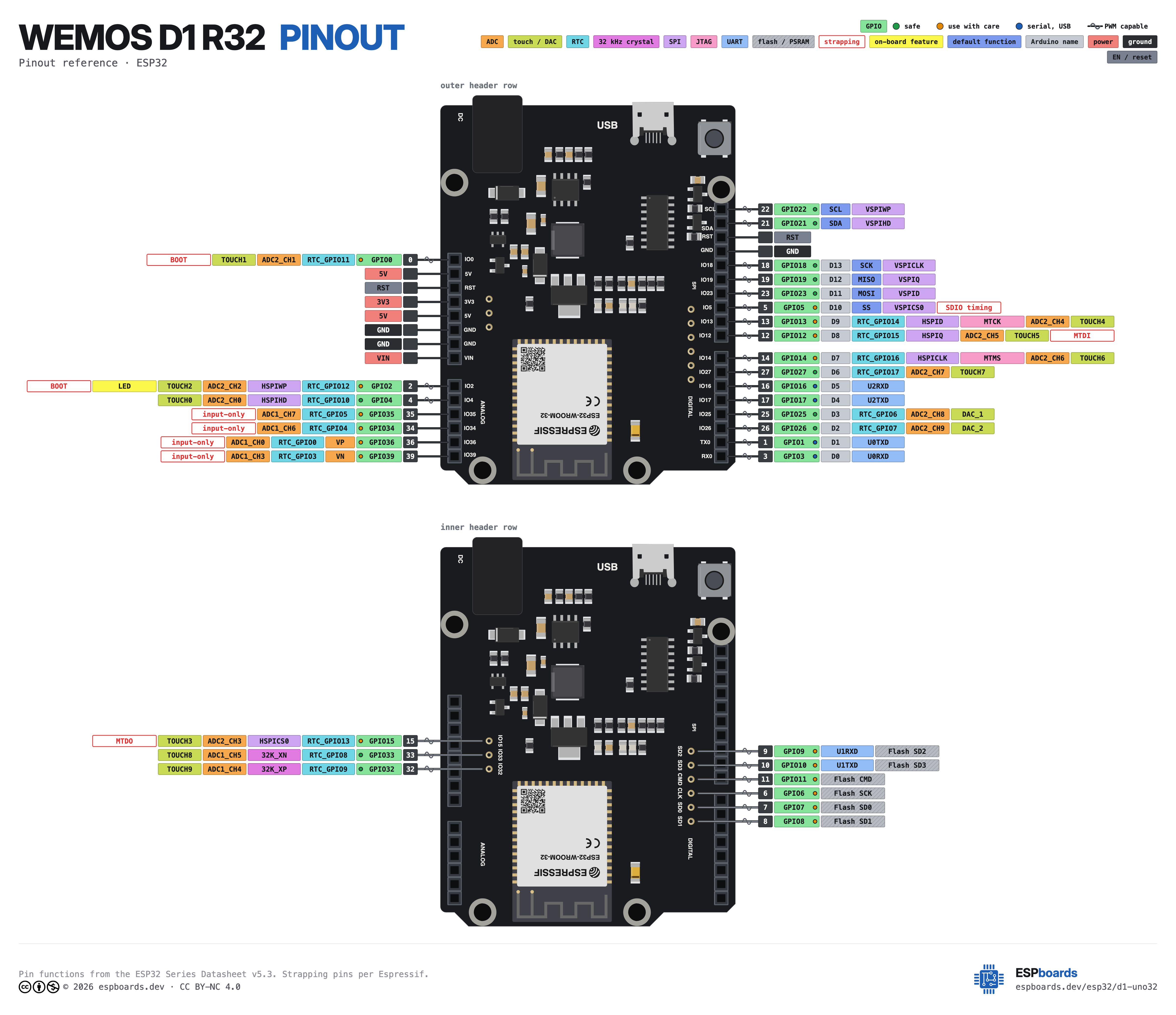
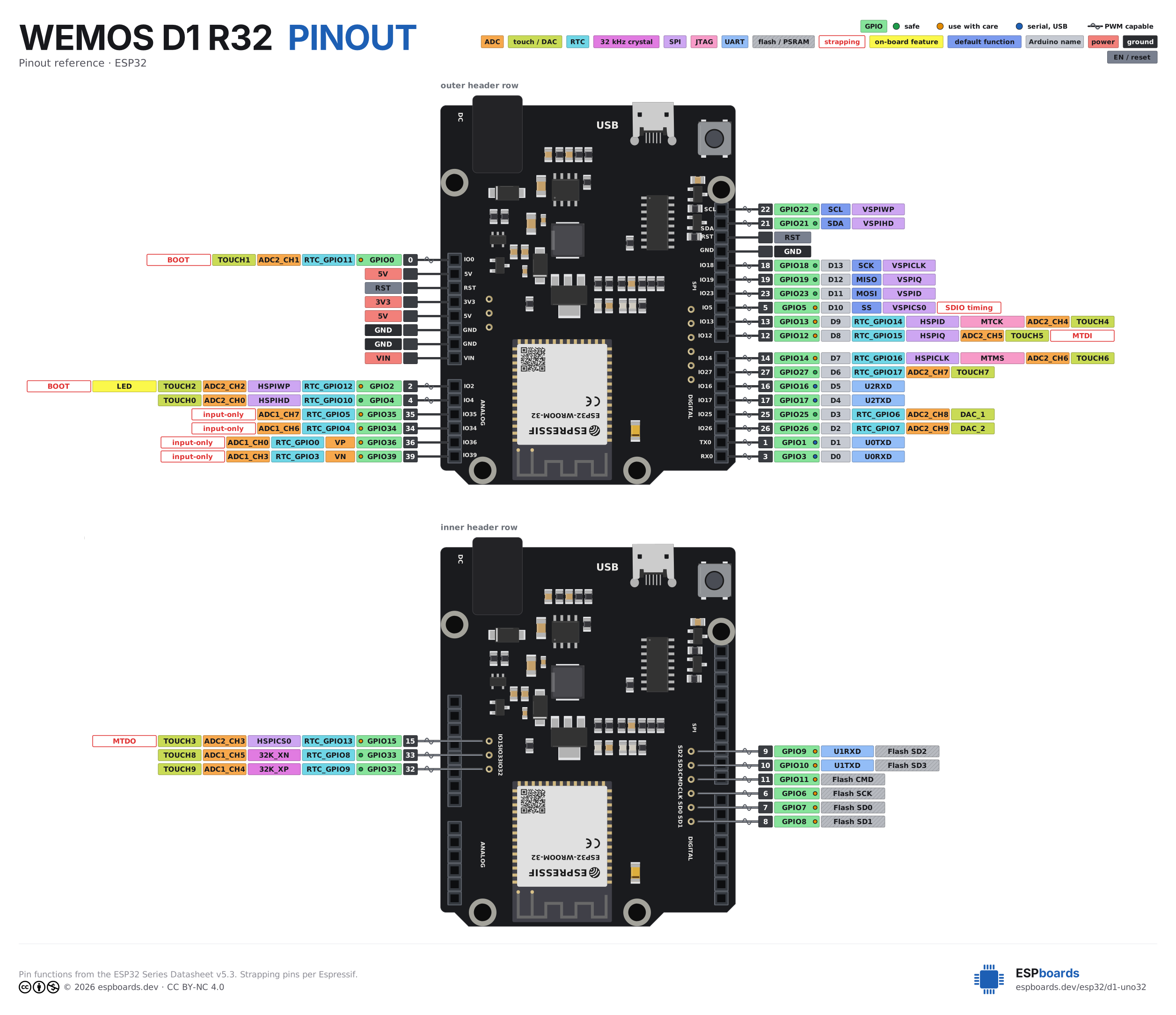
WEMOS D1 R32 Pinout
41 pins · 2.54 mm pitch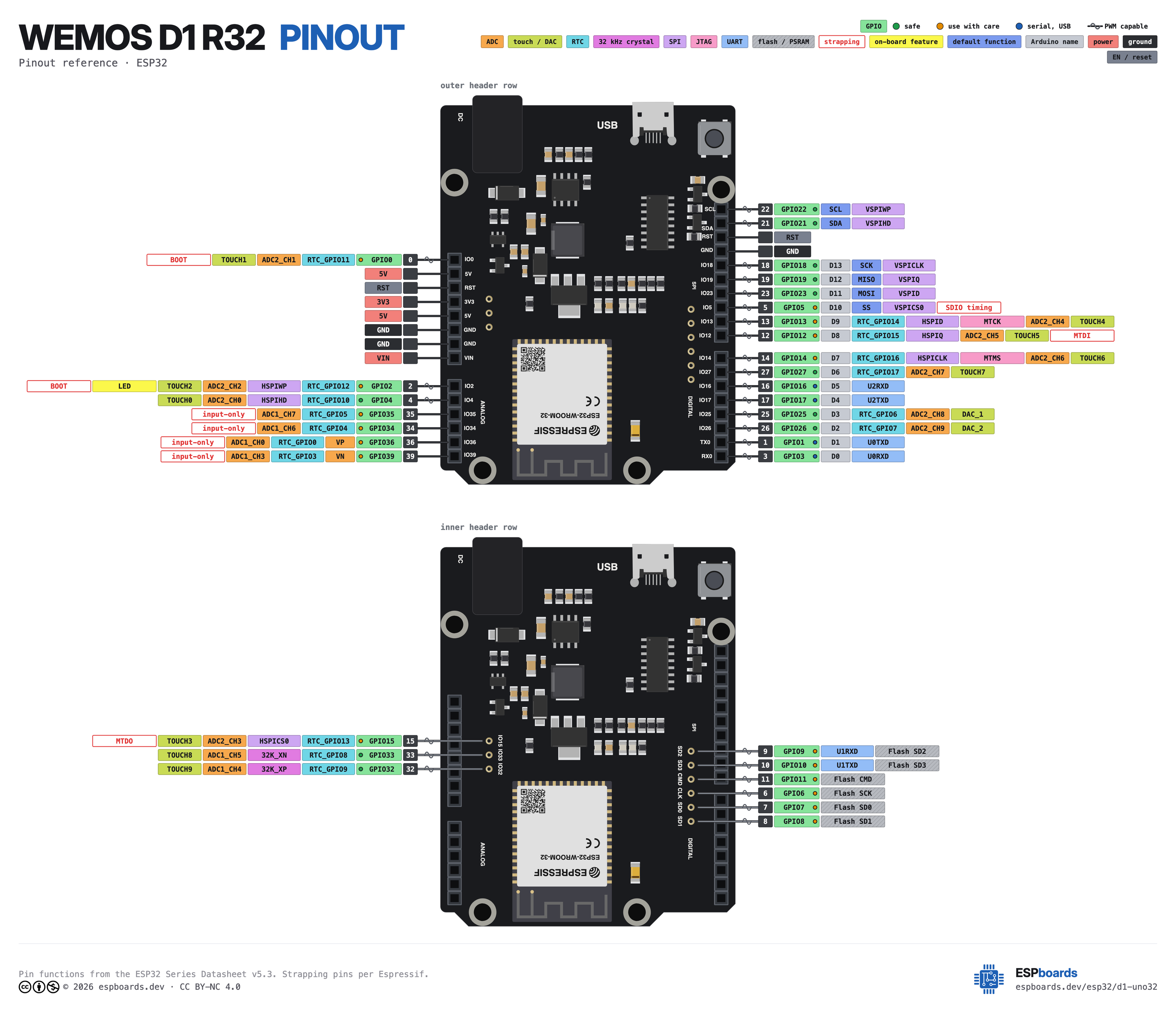
| Pin | GPIO | Labels | Status | Capabilities | Notes |
|---|---|---|---|---|---|
| 1 | 0 | IO0GPIO0 | strapping | adc · touch · pwm | POWER header, the Uno NC position (ETT schematic pin 8, silk IO0). Strapping pin: LOW at reset enters download mode - the CH340 auto-reset drives it, and a shield that ties NC low stops the board booting. ADC2 - analogRead() fails while WiFi is on (use A2-A5, which are ADC1). |
| 2 | - | 5VIOREF | power | - | The Uno IOREF position, wired to 5V here (ETT schematic). A shield that reads IOREF to set its logic level will pick 5V, but GPIOs are 3.3 V only, NOT 5 V tolerant (ESP32 datasheet abs. max VDD + 0.3 V) - 5 V Uno shields need level shifting. |
| 3 | - | RSTEN | control | - | Reset (active LOW), silk RST - the ESP32 EN net shared with the reset button. |
| 4 | - | 3V33.3V | power | - | 3.3 V from the AMS1117 regulator. |
| 5 | - | 5V | power | - | 5 V rail: from USB, or from the MP1482 buck when running on the DC jack. |
| 6 | - | GND | ground | - | Ground |
| 7 | - | GND | ground | - | Ground |
| 8 | - | VIN | power | - | DC jack input (5-12 V per vendor listings), taken before the M7 reverse-polarity diode; feeds the MP1482 buck. |
| 9 | 2 | IO2A0LED_BUILTIN | strapping | adc · touch · pwm | A0 on the Uno header. Blue on-board LED through 1K to GND (ETT schematic). Strapping pin: must be LOW or floating to enter download mode. ADC2 - analogRead() fails while WiFi is on (use A2-A5, which are ADC1). |
| 10 | 4 | IO4A1 | safe | adc · touch · pwm | A1 on the Uno header. ADC2 - analogRead() fails while WiFi is on (use A2-A5, which are ADC1). |
| 11 | 35 | IO35A2 | strapping | adc | A2 on the Uno header. ADC1_CH7; input only, no pull-ups. |
| 12 | 34 | IO34A3 | strapping | adc | A3 on the Uno header. ADC1_CH6; input only, no pull-ups. |
| 13 | 36 | IO36A4VP | strapping | adc | A4 on the Uno header (SENSOR_VP, ADC1_CH0); input only. Uno shields that use A4 as SDA will not work - I2C is on IO21/IO22. |
| 14 | 39 | IO39A5VN | strapping | adc | A5 on the Uno header (SENSOR_VN, ADC1_CH3); input only. Uno shields that use A5 as SCL will not work - I2C is on IO21/IO22. |
| 15 | 22 | IO22SCL | safe | i2c · pwm | Silk SCL, the Uno SCL position. Default I2C SCL. |
| 16 | 21 | IO21SDA | safe | i2c · pwm | Silk SDA, the Uno SDA position. Default I2C SDA. |
| 17 | - | RSTEN | control | - | The Uno AREF position, silk RST on this board (ETT schematic). A shield that drives or decouples AREF lands on reset here, not on an ADC reference. |
| 18 | - | GND | ground | - | Ground |
| 19 | 18 | IO18D13SCK | safe | spi · pwm | D13 on the Uno header. VSPI SCK. |
| 20 | 19 | IO19D12MISO | safe | spi · pwm | D12 on the Uno header. VSPI MISO. |
| 21 | 23 | IO23D11MOSI | safe | spi · pwm | D11 on the Uno header. VSPI MOSI. |
| 22 | 5 | IO5D10SS | strapping | spi · pwm | D10 on the Uno header. VSPI SS. Strapping pin (SDIO timing), outputs a PWM burst at boot. |
| 23 | 13 | IO13D9 | strapping | adc · touch · spi · pwm | D9 on the Uno header. HSPI MOSI. ADC2 - analogRead() fails while WiFi is on (use A2-A5, which are ADC1). |
| 24 | 12 | IO12D8 | strapping | adc · touch · spi · pwm | D8 on the Uno header. Strapping pin (MTDI): pulled HIGH at reset it selects 1.8 V flash and the board will not boot - watch shields with a pull-up on D8. ADC2 - analogRead() fails while WiFi is on (use A2-A5, which are ADC1). |
| 25 | 14 | IO14D7 | strapping | adc · touch · spi · pwm | D7 on the Uno header. HSPI SCK; outputs a PWM burst at boot. ADC2 - analogRead() fails while WiFi is on (use A2-A5, which are ADC1). |
| 26 | 27 | IO27D6 | safe | adc · touch · pwm | D6 on the Uno header. ADC2 - analogRead() fails while WiFi is on (use A2-A5, which are ADC1). |
| 27 | 16 | IO16D5 | uart | uart · pwm | D5 on the Uno header. U2RXD IO_MUX pin: UART2 RX in Arduino core 2.x; core 3.x defaults Serial2 to GPIO4/25, so pass 16 explicitly to Serial2.begin(). |
| 28 | 17 | IO17D4 | uart | uart · pwm | D4 on the Uno header. U2TXD IO_MUX pin: UART2 TX in Arduino core 2.x; core 3.x defaults Serial2 to GPIO4/25, so pass 17 explicitly to Serial2.begin(). |
| 29 | 25 | IO25D3DAC1 | safe | adc · dac · pwm | D3 on the Uno header. DAC1. ADC2 - analogRead() fails while WiFi is on (use A2-A5, which are ADC1). |
| 30 | 26 | IO26D2DAC2 | safe | adc · dac · pwm | D2 on the Uno header. DAC2. ADC2 - analogRead() fails while WiFi is on (use A2-A5, which are ADC1). |
| 31 | 1 | IO1D1TX | uart | uart · pwm | D1 / TX0 on the Uno header: UART0 TX to the CH340C - used for upload and Serial; a shield on D1 can block flashing. |
| 32 | 3 | IO3D0RX | uart | uart · pwm | D0 / RX0 on the Uno header: UART0 RX from the CH340C - used for upload and Serial; a shield on D0 can block flashing. |
| 33 | 15 | IO15 | strapping | adc · touch · spi · pwm | Extra 1 x 3 pad row beside the power header (not an Uno pin; unpopulated). Strapping pin (MTDO): LOW at reset silences boot log output. HSPI SS. ADC2 - analogRead() fails while WiFi is on (use A2-A5, which are ADC1). |
| 34 | 33 | IO33 | safe | adc · touch · pwm | Extra 1 x 3 pad row beside the power header (not an Uno pin; unpopulated). ADC1_CH5 - works with WiFi on. |
| 35 | 32 | IO32 | safe | adc · touch · pwm | Extra 1 x 3 pad row beside the power header (not an Uno pin; unpopulated). ADC1_CH4 - works with WiFi on. |
| 36 | 9 | IO9SD2GPIO9 | strapping | - | Extra 1 x 6 pad row by the digital header, wired to the module's SPI flash - do NOT use, the board will crash or fail to boot. |
| 37 | 10 | IO10SD3GPIO10 | strapping | - | Extra 1 x 6 pad row by the digital header, wired to the module's SPI flash - do NOT use, the board will crash or fail to boot. |
| 38 | 11 | IO11CMDGPIO11 | strapping | - | Extra 1 x 6 pad row by the digital header, wired to the module's SPI flash - do NOT use, the board will crash or fail to boot. |
| 39 | 6 | IO6CLKGPIO6 | strapping | - | Extra 1 x 6 pad row by the digital header, wired to the module's SPI flash - do NOT use, the board will crash or fail to boot. |
| 40 | 7 | IO7SD0GPIO7 | strapping | - | Extra 1 x 6 pad row by the digital header, wired to the module's SPI flash - do NOT use, the board will crash or fail to boot. |
| 41 | 8 | IO8SD1GPIO8 | strapping | - | Extra 1 x 6 pad row by the digital header, wired to the module's SPI flash - do NOT use, the board will crash or fail to boot. |
Start with these
13 pins with no boot or system involvementFreely assignable - no strapping, flash, USB or JTAG duties. Ideal first picks for buttons, sensors and LEDs.
Fine - with a little care
13 pins · 11 things to knowIO0 Bootstrapping pin (enter bootloader when low); internal pull-up. Strapping
Must be HIGH during boot for normal startup; if held LOW on reset, forces flash programming mode.
IO2 Bootstrapping pin (must be low or floating at reset); internal pull-down. Strapping
If driven HIGH on reset (while IO0 is LOW), selects an unsupported SDIO boot mode, causing boot failure.
IO35IO39 Input-only GPIOs with ADC1 channels - no output driver Other
Cannot be used as output; only suitable for input.
- IO35Input-only GPIO (no output driver); ADC1 channel 7.
- IO39Input-only GPIO (no output); ADC1 channel 3, Hall sensor VN.
IO34 Input-only GPIO (no output driver); ADC1 channel 6. Other
Cannot be used as output (no drive capability); only suitable for analog/digital input.
IO36 Input-only GPIO (no output); ADC1 channel 0, Hall sensor VP. Other
Cannot be used as output; only suitable for input (e.g., analog read).
IO5 Bootstrapping pin; internal pull-up; VSPI CS0 (default SPI chip-select); acts as FSPIWP (flash write-protect) on internal-flash variants. Strapping
Must be HIGH during boot; if pulled LOW at reset, alters SDIO slave timing and may prevent normal boot.
IO13 JTAG clock pin (TCK); also ADC2 channel 4 / Touch4 input. JTAG
Used for JTAG debugging (TCK); avoid using as GPIO if JTAG is needed.
IO12 Bootstrapping pin; JTAG TDI; sets flash voltage (VDD_SDIO); also HSPIQ (flash data line). Strapping
Keep LOW during boot (internal PD); pulling HIGH at reset selects 1.8V flash mode, causing flash brownout if 3.3V flash is used.
IO14 JTAG mode select pin (TMS); also HSPI CLK and PWM-capable GPIO. JTAG
Used for JTAG debugging (TMS); driving it as GPIO may interfere with JTAG or produce spurious signals at boot.
IO1IO3 Used by the CH340C USB serial bridge onboard hardware
Wired to the CH340C USB serial bridge on this board. The pin is yours if you give that up, but nothing else can share it.
- IO1D1 / TX0 on the Uno header: UART0 TX to the CH340C - used for upload and Serial; a shield on D1 can block flashing.
- IO3D0 / RX0 on the Uno header: UART0 RX from the CH340C - used for upload and Serial; a shield on D0 can block flashing.
IO15 Bootstrapping pin; JTAG TDO; controls UART0 boot log output; also HSPICS0 (secondary SPI CS). Strapping
Keep HIGH during boot (internal PU); if LOW on reset, bootloader log is silenced and boot mode may change.
Only if you know the tricks
6 pins · 4 things to knowIO9IO10 SPI flash/PSRAM data lines SD2 and SD3 (flash HOLD and WP) Flash
Used by internal flash/PSRAM; typically not exposed on modules, avoid using as GPIO.
- IO9Connected to SPI flash/PSRAM data 2 (SD2, flash HOLD).
- IO10Connected to SPI flash/PSRAM data 3 (SD3, flash WP).
IO11 Connected to SPI flash command/CS (CMD/CS0). Flash
Used by internal flash (chip select/command); not available for general use.
IO6 Connected to SPI flash clock (SCK/CLK). Flash
Used for internal flash/PSRAM communication; not available for general GPIO.
IO7IO8 SPI flash data lines SD0 and SD1 Flash
Used for internal flash/PSRAM data; not available for general GPIO.
- IO7Connected to SPI flash data 0 (SD0).
- IO8Connected to SPI flash data 1 (SD1).
The WEMOS D1 R32 breaks out 41 pins in total: 32 GPIO for your project, with 5V, 3V3, GND and VIN handling power.
Peripheral wiring is straightforward: I²C is mapped to SDA on GPIO21 and SCL on GPIO22; the SPI bus (MOSI, MISO, SCK, SS) is broken out in full; TX/RX on GPIO1 and GPIO3 cover serial logging and flashing.
Beyond plain digital I/O you get 16 ADC-capable pins for sensors and battery monitoring, PWM on 22 pins, 10 capacitive-touch inputs and 2 true DAC outputs.
13 of the exposed pins carry boot-time or system duties on the ESP32 (IO0, IO2, IO35 and 10 more) - check the guidance above before wiring anything to them. IO4, IO22, IO21, IO18 and 9 more are free of any such role - the safest first picks.
Getting started
flash your first firmware in ~2 minutesBoard: ESP32 Dev Module Flash Size: 4MB (32Mb) Flash Mode: DIO Partition Scheme: Default 4MB with spiffs (1.2MB APP/1.5MB SPIFFS) Upload Speed: 921600
// toggle GPIO4 - wire an LED and resistor to it
void setup() {
  pinMode(4, OUTPUT);
}
void loop() {
  digitalWrite(4, HIGH); delay(500);
  digitalWrite(4, LOW);  delay(500);
}[env:d1_uno32]
platform = espressif32
board = esp32dev
framework = arduino
monitor_speed = 115200
upload_speed = 921600esp32dev - or type it after board =.esp32:
board: esp32dev
variant: esp32
framework:
type: esp-idf
# blink - GPIO4
output:
- platform: gpio
pin: 4
id: led_out
light:
- platform: binary
name: "LED"
output: led_outesp32dev (same ids as PlatformIO).esptool.py --chip esp32 --port /dev/ttyACM0 \
--baud 921600 write_flash 0x1000 firmware.bin--port = your /dev/tty* (macOS/Linux) or COMx (Windows).Downloads
Free for non-commercial use, credit espboards.dev · License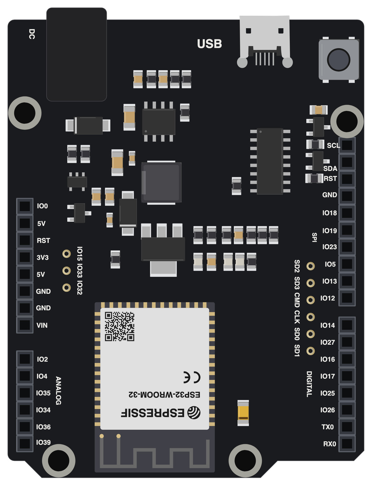
Board illustration
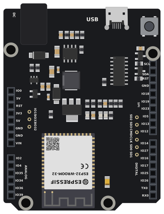
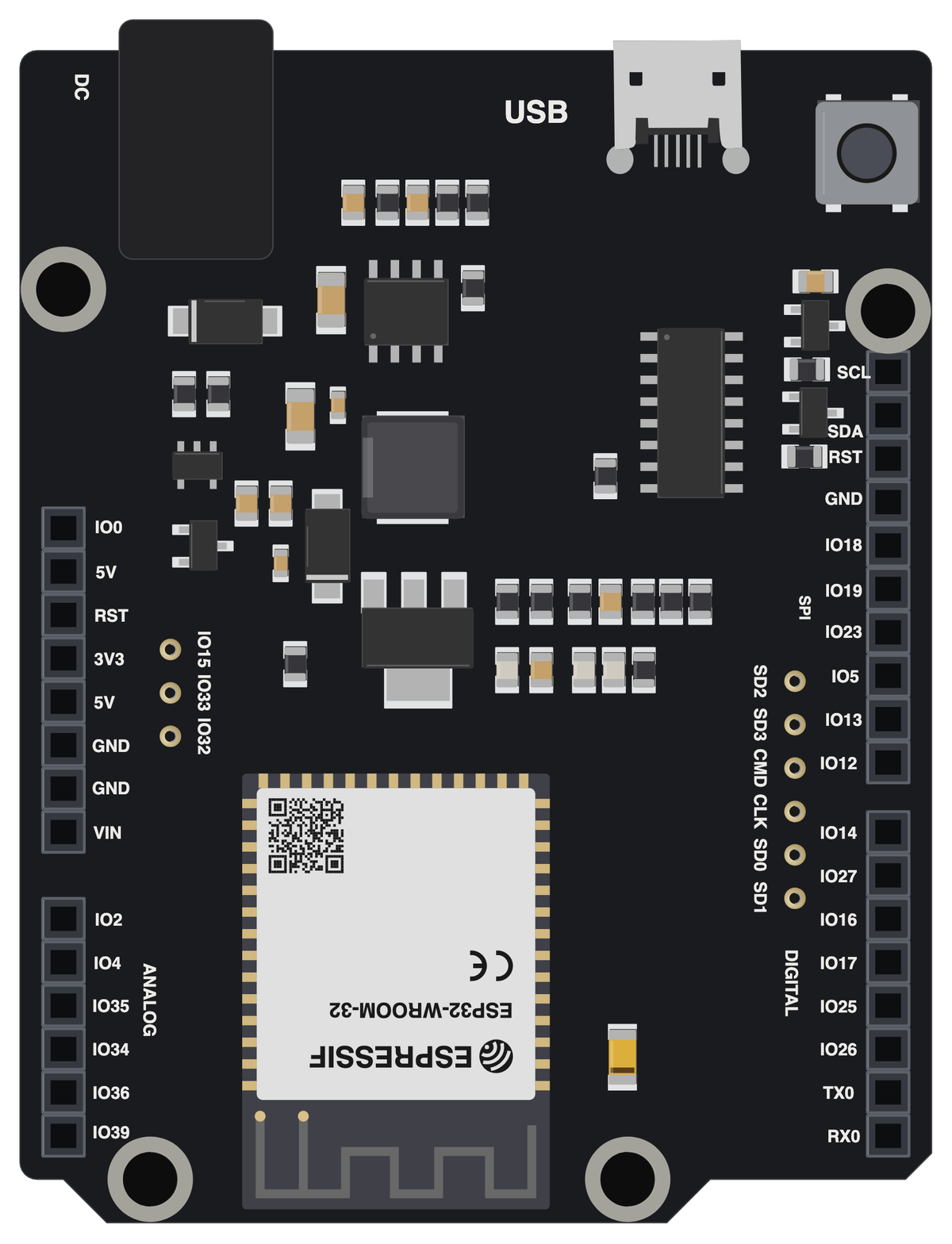
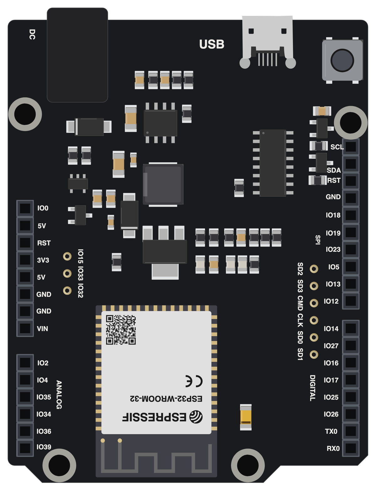
The bare WEMOS D1 R32 board drawn to scale at 68.58 × 53.34 mm, with no pin labels on it. Made for slide decks, wiring diagrams and project write-ups where a photo is too busy. Take the scalable SVG for print or editing, the high-resolution PNG to drop straight in, or the transparent PNG when you need it with no background behind it.
Pinout diagram
Every pin on both sides of the board with its functions, drawn by ESPboards from the ESP32 Series Datasheet v5.3 - the same sheet shown at the top of this page. The PNG is a high-resolution image for screens, the SVG is vector so it stays sharp at any size, and the PDF is laid out to print on A4 or Letter.
Yours to use, share and adapt for non-commercial work, as long as you credit espboards.dev - the full terms and ready-made credit lines are here.
Specifications
ESP32 · 68.58 × 53.34 mm · vs other ESP32 chips →Dimensions

About this board
Inside sits the ESP32 - a dual-core Xtensa with both Bluetooth Classic and BLE.
With 32 GPIO broken out, you get more pins to play with than most ESP32 boards offer.
Around the module: status LEDs (Power, User (GPIO2)) and Reset buttons.
Resources
Similar boards


