
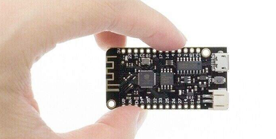
WEMOS LOLIN32 Lite is a development board based on the ESP32 microcontroller using XTENSA architecture.
This board features a maximum CPU frequency of 240 MHz and 4MB flash memory.
About WEMOS LOLIN32 Lite
The WEMOS LOLIN32 Lite squeezes Espressif’s dual-core ESP32-WROOM-32 module into a slim 57 × 25 mm board that still accepts the classic LOLIN/D1-mini shield ecosystem. It ships with 4 MB of flash, runs up to 240 MHz, and offers both Wi-Fi 802.11 b/g/n and Bluetooth 4.2 (BR/EDR + BLE) for rock-solid wireless connectivity. 📡
A low-cost CH340C USB-to-UART bridge handles programming and serial debugging via the Micro-USB port and supports auto-reset/boot so you can flash sketches without pushing buttons. :contentReference
Onboard power management is Li-Po ready: a TP4054 charger (≈ 500 mA) and a PH-2 battery connector (BAT) let you run projects untethered while the board trickle-charges whenever USB is present. ⚡️
Convenience extras include a RESET push-button, a BOOT (IO0) button for manual download-mode entry, and a bright blue on-board LED on GPIO 5 for quick status indication.
With 22 GPIOs (all PWM-capable), 12-bit ADCs, dual 8-bit DACs, 10 capacitive-touch pads, plus I²C, SPI, UART, SD-card, and RTC IO support, the LOLIN32 Lite punches far above its weight for battery-powered IoT nodes, wearables, or compact sensor gateways. ⚙️
Where to Buy WEMOS LOLIN32 Lite

Starting from
$5 per unit


Prices are subject to change. We earn from qualifying purchases as an Amazon Associate.
Technical Specifications
Complete technical specification details for WEMOS LOLIN32 Lite
USB
Connectivity
Microcontroller
✨ Features & Pins
Quick Setup
Copy-paste configs for WEMOS LOLIN32 Lite - auto‑generated from this board's exact hardware specs.
In Arduino IDE 2 select Lolin32 Lite from the esp32 by Espressif package. In PlatformIO use board = esp32dev. ESP32 · 240 MHz · 4MB · DIO.
In Arduino IDE 2, open Boards Manager, search "esp32" by Espressif and install it. Then go to Tools → Board and select "Lolin32 Lite" for the WEMOS LOLIN32 Lite.
WEMOS LOLIN32 Lite Board Dimensions
Physical measurements for WEMOS LOLIN32 Lite
WEMOS LOLIN32 Lite Pinout Diagram
Complete pin reference for WEMOS LOLIN32 Lite
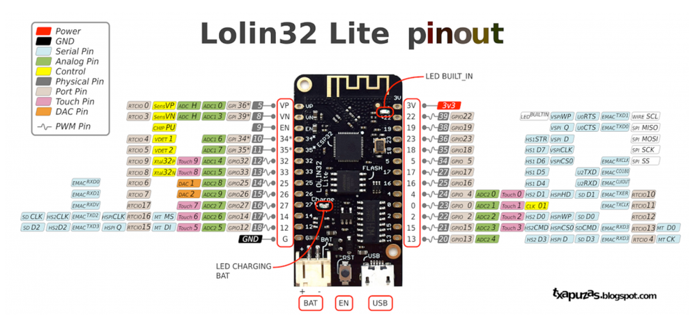
The LOLIN32 Lite pinout fans out 26 ESP32 GPIOs on two rows, mirroring the original D1-mini shield headers for easy stacking.
Power rails: use USB 5V (or VIN) as input, the regulated 3V3 pin for logic-level peripherals, and the dedicated BAT pin for a single-cell Li-Po. Multiple GND pads provide solid returns.
Serial: U0_TX (GPIO1) and U0_RX (GPIO3) connect to the CH340C for programming/logging. Need more ports? U2_TX (GPIO17) and U2_RX (GPIO16) are free for GPS or RS-485 transceivers.
I²C defaults to SDA (GPIO21) and SCL (GPIO22), broken out on the shield D2/D1 lines-but any spare GPIO can be reassigned.
SPI: the primary VSPI bus (best for OLEDs, SD adapters, radios) maps to MOSI (GPIO23), MISO (GPIO19), SCK (GPIO18), and CS (GPIO5). A secondary HSPI bus lives on GPIO12-15 when you need a second device.
Analog & touch: Eight ADC1 channels (GPIO32-GPIO39) work even with Wi-Fi on. Extra ADC2 pads (GPIO0, 2, 4, 12-15, 25-27) share RF hardware. Dual 8-bit DAC outputs are on GPIO25 and GPIO26. Ten pads double as capacitive-touch inputs-great for touch keys or wake-up gestures.
Every GPIO can generate high-resolution PWM (up to ≈40 kHz). Remember the boot-strap pins-GPIO0, GPIO2, and GPIO15-must sit HIGH (with proper pull-ups) on reset for a normal boot.
With battery charging, robust power rails, and a shield-friendly layout, the LOLIN32 Lite pinout makes it effortless to go from breadboard prototype to compact, battery-powered product.
Safe Pins to Use
These pins are safe for general GPIO usage without boot or system conflicts
Why Are These Pins Safe?
Pins to Avoid or Use with Caution
Reserved for critical functions. Misuse may cause boot failures, programming issues, or system conflicts.
Boot behavior & flash voltage
Low-level debugging interface
USB Serial/JTAG communication
Memory & PSRAM connections
Debugging & firmware uploads
| PIN | Label | Why Avoid | Type |
|---|---|---|---|
| IO0 | GPIO0 | Must be HIGH during boot for normal startup; if held LOW on reset, forces flash programming mode. | 🛠️ Strapping |
| IO2 | GPIO2 | If driven HIGH on reset (while IO0 is LOW), selects an unsupported SDIO boot mode, causing boot failure. | 🛠️ Strapping |
| IO4 | GPIO4 | Sampled at reset for boot config; should not be driven at boot (affects boot mode timing). | 🛠️ Strapping |
| IO5 | GPIO5 | Must be HIGH during boot; if pulled LOW at reset, alters SDIO slave timing and may prevent normal boot. | 🛠️ Strapping |
| IO12 | MTDI (GPIO12) | Keep LOW during boot (internal PD); pulling HIGH at reset selects 1.8V flash mode, causing flash brownout if 3.3V flash is used. | 🛠️ Strapping |
| IO13 | MTCK (GPIO13) | Used for JTAG debugging (TCK); avoid using as GPIO if JTAG is needed. | 🪛 Other |
| IO14 | MTMS (GPIO14) | Used for JTAG debugging (TMS); driving it as GPIO may interfere with JTAG or produce spurious signals at boot. | 🪛 Other |
| IO15 | MTDO (GPIO15) | Keep HIGH during boot (internal PU); if LOW on reset, bootloader log is silenced and boot mode may change. | 🛠️ Strapping |
| IO16 | GPIO16 | Connected to internal PSRAM on PSRAM-enabled modules; not usable as GPIO on those modules. | ⚡ Flash |
| IO17 | GPIO17 | Connected to internal PSRAM on PSRAM-enabled modules; not usable as GPIO on those modules. | ⚡ Flash |
| IO34 | GPIO34 | Cannot be used as output (no drive capability); only suitable for analog/digital input. | 🪛 Other |
| IO35 | GPIO35 | Cannot be used as output; only suitable for input. | 🪛 Other |
| IO36 | GPIO36 (SENSOR_VP) | Cannot be used as output; only suitable for input (e.g., analog read). | 🪛 Other |
| IO39 | GPIO39 (SENSOR_VN) | Cannot be used as output; only suitable for input. | 🪛 Other |
Useful Links
Datasheets and resources for WEMOS LOLIN32 Lite
WEMOS LOLIN32 Lite Custom Pin Mapping
Pin configuration and GPIO mapping for WEMOS LOLIN32 Lite
| Pin | Function | ESP Pin | I/O Type | Description |
|---|---|---|---|---|
| 1 | 5V | 5V | POWER INPUT | 5V power input for the board |
| 2 | GND | GND | POWER GROUNT | Ground connection |
| 3 | 3V3 | 3.3V | POWER OUTPUT | 3.3V power output |
| 5 | IO0 | GPIO0 | BIDIRECTIONAL | GPIO, ADC |
| 6 | IO2 | GPIO2 | BIDIRECTIONAL | GPIO, ADC |
| 7 | IO4 | GPIO4 | BIDIRECTIONAL | GPIO, ADC |
| 8 | IO5 | GPIO5 | BIDIRECTIONAL | GPIO |
| 9 | IO12 | GPIO12 | BIDIRECTIONAL | GPIO, ADC |
| 10 | IO13 | GPIO13 | BIDIRECTIONAL | GPIO, ADC |
| 11 | IO14 | GPIO14 | BIDIRECTIONAL | GPIO, ADC |
| 12 | IO15 | GPIO15 | BIDIRECTIONAL | GPIO |
| 13 | IO16 | GPIO16 | BIDIRECTIONAL | GPIO |
| 14 | IO17 | GPIO17 | BIDIRECTIONAL | GPIO |
| 15 | IO18 | GPIO18 | BIDIRECTIONAL | GPIO |
| 16 | IO19 | GPIO19 | BIDIRECTIONAL | GPIO |
| 17 | IO22 | GPIO22 | BIDIRECTIONAL | GPIO |
| 18 | IO23 | GPIO23 | BIDIRECTIONAL | GPIO |
| 19 | IO25 | GPIO25 | BIDIRECTIONAL | GPIO, ADC |
| 20 | IO26 | GPIO26 | BIDIRECTIONAL | GPIO, ADC |
| 21 | IO27 | GPIO27 | BIDIRECTIONAL | GPIO, ADC |
| 22 | IO32 | GPIO32 | BIDIRECTIONAL | GPIO, ADC |
| 23 | IO33 | GPIO33 | BIDIRECTIONAL | GPIO, ADC |
| 24 | IO34 | GPIO34 | BIDIRECTIONAL | GPIO, ADC |
| 25 | IO35 | GPIO35 | BIDIRECTIONAL | GPIO, ADC |
| 26 | IO36 | GPIO36 | BIDIRECTIONAL | GPIO, ADC |
| 27 | IO39 | GPIO39 | BIDIRECTIONAL | GPIO, ADC |
Pin Mappings
Complete pinout and GPIO mapping for WEMOS LOLIN32 Lite
| Pin | Analog | Touch | PWM | Other |
|---|---|---|---|---|
| 0 | A11 | T1 | ||
| 1 | PWM | TX | ||
| 2 | A12 | T2 | PWM | |
| 3 | PWM | RX | ||
| 4 | A10 | T0 | PWM | |
| 5 | PWM | SS | ||
| 12 | A15 | T5 | PWM | |
| 13 | A14 | T4 | PWM | |
| 14 | A16 | T6 | PWM | |
| 15 | A13 | T3 | PWM | |
| 18 | PWM | SCK | ||
| 19 | PWM | SDA MISO | ||
| 22 | PWM | LED_BUILTIN | ||
| 23 | PWM | SCL MOSI | ||
| 25 | A18 | PWM | DAC1 | |
| 26 | A19 | PWM | DAC2 | |
| 27 | A17 | T7 | PWM | |
| 32 | A4 | T9 | PWM | |
| 33 | A5 | T8 | PWM | |
| 34 | A6 | |||
| 35 | A7 | |||
| 36 | A0 | |||
| 39 | A3 |
Default Tools & Configuration
Build and upload settings for WEMOS LOLIN32 Lite
| Setting | Value |
|---|---|
| Bootloader tool | esptool_py |
| Uploader tool | esptool_py |
| Network uploader tool | esp_ota |
| Bootloader address | 0x1000 |
| Flash mode | dio |
| Boot mode | dio |
| Maximum upload size | 1280 KB (1310720 bytes) |
| Maximum data size | 320 KB (327680 bytes) |
The WEMOS LOLIN32 Lite uses esptool_py for uploads , esp_ota for OTA updates, and esptool_py bootloader at 0x1000.
Flash mode: dio | Boot mode: dio
Max sketch size: 1280 KB | Max data size: 320 KB
Similar Boards
Other development boards with ESP32 microcontroller

WeMos WiFi&Bluetooth Battery
WeMos WiFi&Bluetooth Battery development board is based on esp32 microcontroller and uses xtensa architecture.

WEMOS LOLIN32
WEMOS LOLIN32 development board is based on esp32 microcontroller and uses xtensa architecture.

LOLIN C3 Mini
LOLIN C3 Mini development board is based on esp32c3 microcontroller and uses riscv32 architecture.