
M5Stack-Timer-CAM
ESP32 board with built-in camera and LiPo support - perfect for low-power time-lapse and surveillance apps.

M5Stack-Timer-CAM Pinout
30 pins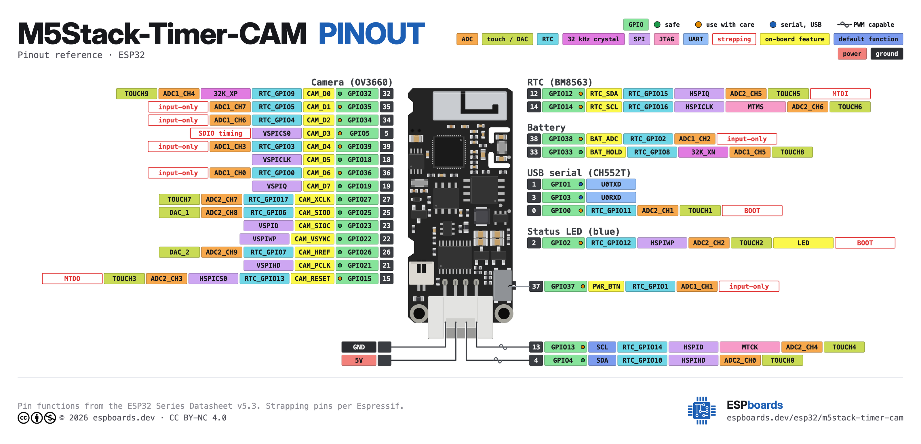
| Pin | GPIO | Labels | Status | Capabilities | Notes |
|---|---|---|---|---|---|
| 1 | 13 | G13SCL | strapping | i2c · adc · touch · pwm | Grove port (HY2.0-4P) pin 1, SCL. One of only two GPIOs brought out; 22R series resistor and an ESD diode on the board |
| 2 | 4 | G4SDA | safe | i2c · adc · touch · pwm | Grove port (HY2.0-4P) pin 2, SDA. One of only two GPIOs brought out; 22R series resistor and an ESD diode on the board |
| 3 | - | 5VVSYS | power | - | Grove port pin 3. The VSYS rail: USB 5V or the battery, each through a Schottky diode, so a little under 5V on USB and battery voltage on the LiPo |
| 4 | - | GND | ground | - | Grove port pin 4 |
| 5 | 32 | CAM_D0 | safe | - | Camera data bit 0 (Y2) |
| 6 | 35 | CAM_D1 | strapping | - | Camera data bit 1 (Y3) |
| 7 | 34 | CAM_D2 | strapping | - | Camera data bit 2 (Y4) |
| 8 | 5 | CAM_D3 | strapping | - | Camera data bit 3 (Y5) |
| 9 | 39 | CAM_D4 | strapping | - | Camera data bit 4 (Y6) |
| 10 | 18 | CAM_D5 | safe | - | Camera data bit 5 (Y7) |
| 11 | 36 | CAM_D6 | strapping | - | Camera data bit 6 (Y8) |
| 12 | 19 | CAM_D7 | safe | - | Camera data bit 7 (Y9) |
| 13 | 27 | CAM_XCLK | safe | - | Camera system clock (XCLK) |
| 14 | 25 | CAM_SIOD | safe | - | Camera SCCB data (SIOD), 2K pull-up |
| 15 | 23 | CAM_SIOC | safe | - | Camera SCCB clock (SIOC), 2K pull-up |
| 16 | 22 | CAM_VSYNC | safe | - | Camera vertical sync (VSYNC) |
| 17 | 26 | CAM_HREF | safe | - | Camera horizontal reference (HREF) |
| 18 | 21 | CAM_PCLK | safe | - | Camera pixel clock (PCLK) |
| 19 | 15 | CAM_RESET | strapping | - | Camera reset (RESET); PWDN is not wired (-1) |
| 20 | 12 | RTC_SDA | strapping | - | I2C data to the BM8563 real-time clock. Also a strapping pin (MTDI) |
| 21 | 14 | RTC_SCL | strapping | - | I2C clock to the BM8563 real-time clock |
| 22 | 38 | BAT_ADC | strapping | - | Battery voltage through a 1.37K / 2.67K divider (battery = reading x 1.51). Input-only |
| 23 | 33 | BAT_HOLD | safe | - | Battery power latch: drive HIGH early in setup to keep running on the LiPo after the PWR button is released; LOW switches the board off on battery |
| 24 | 37 | PWR_BTN | strapping | - | Reads the PWR/WAKE side button through a diode (low while pressed). Input-only; from the schematic, not in the M5Stack pin table |
| 25 | 2 | LED_BUILTINLED | strapping | - | Blue status LED (470R to GND), lit HIGH. Also a strapping pin |
| 26 | 0 | G0BOOT | strapping | - | Download-mode strap, pulled low by the CH552T USB bridge for auto-upload. No BOOT button; also on the front G0 test pad |
| 27 | 1 | TXDU0TXD | uart | uart | UART0 TX to the CH552T USB bridge; also on the front TXD test pad |
| 28 | 3 | RXDU0RXD | uart | uart | UART0 RX from the CH552T USB bridge |
| 29 | 16 | PSRAM_CS | strapping | - | PSRAM chip select |
| 30 | 17 | PSRAM_CLK | strapping | - | PSRAM clock |
Start with these
1 pins with no boot or system involvementFreely assignable - no strapping, flash, USB or JTAG duties. Ideal first picks for buttons, sensors and LEDs.
Fine - with a little care
5 pins · 4 things to knowG13GPIO13 JTAG clock pin (TCK); also ADC2 channel 4 / Touch4 input. JTAG
Used for JTAG debugging (TCK); avoid using as GPIO if JTAG is needed.
LED_BUILTINGPIO2 Blue status LED (470R to GND), lit HIGH. Also a strapping pin onboard hardware
Wired to the blue status LED on this board. The pin is yours if you give that up, but nothing else can share it.
G0GPIO0 Download-mode strap, pulled low by the CH552T USB bridge for auto-upload. No BOOT button; also on the front G0 test pad onboard hardware
Wired to the USB serial bridge (auto-download) on this board. The pin is yours if you give that up, but nothing else can share it.
TXDGPIO1RXDGPIO3 Used by the USB serial bridge (CH552T) onboard hardware
Wired to the USB serial bridge (CH552T) on this board. The pin is yours if you give that up, but nothing else can share it.
- TXDUART0 TX to the CH552T USB bridge; also on the front TXD test pad
- RXDUART0 RX from the CH552T USB bridge
Only if you know the tricks
22 pins · 6 things to knowCAM_D0GPIO32CAM_D1GPIO35CAM_D2GPIO34CAM_D3GPIO5CAM_D4GPIO39CAM_D5GPIO18CAM_D6GPIO36CAM_D7GPIO19CAM_XCLKGPIO27CAM_SIODGPIO25CAM_SIOCGPIO23CAM_VSYNCGPIO22CAM_HREFGPIO26CAM_PCLKGPIO21CAM_RESETGPIO15 Used by the OV3660 camera onboard hardware
Wired to the OV3660 camera on this board, which is soldered down. Driving it from your own code breaks that function.
- CAM_D0Camera data bit 0 (Y2)
- CAM_D1Camera data bit 1 (Y3)
- CAM_D2Camera data bit 2 (Y4)
- CAM_D3Camera data bit 3 (Y5)
- CAM_D4Camera data bit 4 (Y6)
- CAM_D5Camera data bit 5 (Y7)
- CAM_D6Camera data bit 6 (Y8)
- CAM_D7Camera data bit 7 (Y9)
- CAM_XCLKCamera system clock (XCLK)
- CAM_SIODCamera SCCB data (SIOD), 2K pull-up
- CAM_SIOCCamera SCCB clock (SIOC), 2K pull-up
- CAM_VSYNCCamera vertical sync (VSYNC)
- CAM_HREFCamera horizontal reference (HREF)
- CAM_PCLKCamera pixel clock (PCLK)
- CAM_RESETCamera reset (RESET); PWDN is not wired (-1)
RTC_SDAGPIO12RTC_SCLGPIO14 Used by the BM8563 RTC onboard hardware
Wired to the BM8563 RTC on this board, which is soldered down. Driving it from your own code breaks that function.
- RTC_SDAI2C data to the BM8563 real-time clock. Also a strapping pin (MTDI)
- RTC_SCLI2C clock to the BM8563 real-time clock
BAT_ADCGPIO38 Battery voltage through a 1.37K / 2.67K divider (battery = reading x 1.51). Input-only onboard hardware
Wired to the battery voltage divider on this board, which is soldered down. Driving it from your own code breaks that function.
BAT_HOLDGPIO33 Battery power latch: drive HIGH early in setup to keep running on the LiPo after the PWR button is released; LOW switches the board off on battery onboard hardware
Wired to the battery power latch on this board, which is soldered down. Driving it from your own code breaks that function.
PWR_BTNGPIO37 Reads the PWR/WAKE side button through a diode (low while pressed). Input-only; from the schematic, not in the M5Stack pin table onboard hardware
Wired to the PWR/WAKE button on this board, which is soldered down. Driving it from your own code breaks that function.
PSRAM_CSGPIO16PSRAM_CLKGPIO17 Used by the 8MB PSRAM onboard hardware
Wired to the 8MB PSRAM on this board, which is soldered down. Driving it from your own code breaks that function.
- PSRAM_CSPSRAM chip select
- PSRAM_CLKPSRAM clock
Across 30 pins, the M5Stack-Timer-CAM exposes 28 GPIO plus 5V and GND for power.
For peripherals, I²C is mapped to SDA on GPIO4 and SCL on GPIO13.
On the analog side there are 2 ADC-capable pins for sensors and battery monitoring, PWM on 2 pins and 2 capacitive-touch inputs.
If you want zero surprises, G4 is free of any such role - the safest first picks. 5 of the exposed pins carry boot-time or system duties on the ESP32 (G13, LED_BUILTIN, G0 and 2 more).
Getting started
flash your first firmware in ~2 minutesBoard: ESP32 Wrover Module Flash Size: 4MB (32Mb) Flash Mode: DIO PSRAM: QSPI PSRAM Partition Scheme: Default 4MB with spiffs (1.2MB APP/1.5MB SPIFFS) Upload Speed: 921600
// toggle GPIO4 - wire an LED and resistor to it
void setup() {
  pinMode(4, OUTPUT);
}
void loop() {
  digitalWrite(4, HIGH); delay(500);
  digitalWrite(4, LOW);  delay(500);
}[env:m5stack-timer-cam]
platform = espressif32
board = esp32dev
framework = arduino
monitor_speed = 115200
upload_speed = 921600
board_build.arduino.memory_type = qio_qspi
build_flags = -DBOARD_HAS_PSRAMesp32dev - or type it after board =.esp32:
board: esp32dev
variant: esp32
framework:
type: esp-idf
psram:
mode: quad
speed: 80MHz
# blink - GPIO4
output:
- platform: gpio
pin: 4
id: led_out
light:
- platform: binary
name: "LED"
output: led_outesp32dev (same ids as PlatformIO).esptool.py --chip esp32 --port /dev/ttyACM0 \
--baud 921600 write_flash 0x1000 firmware.bin--port = your /dev/tty* (macOS/Linux) or COMx (Windows).Downloads
Free for non-commercial use, credit espboards.dev · License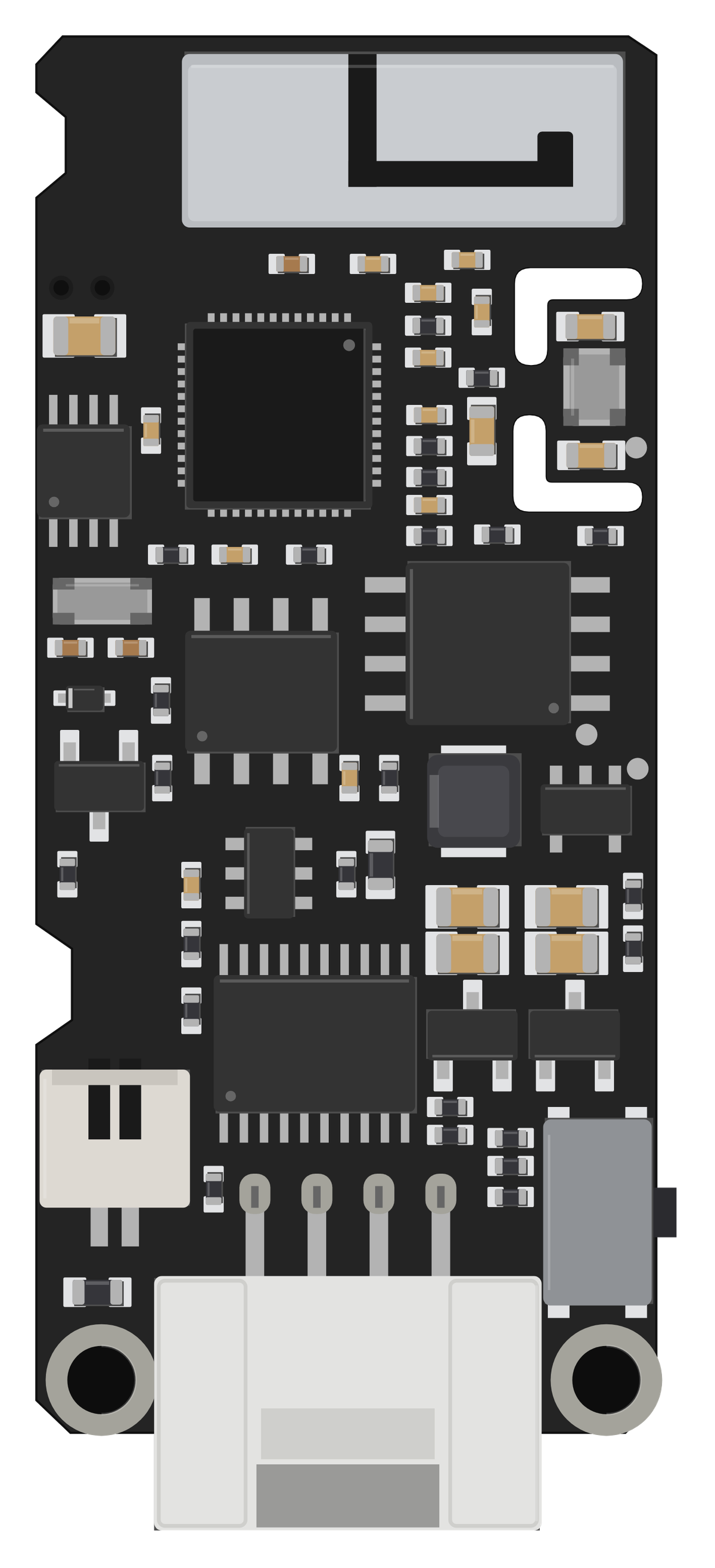
Board illustration
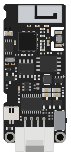
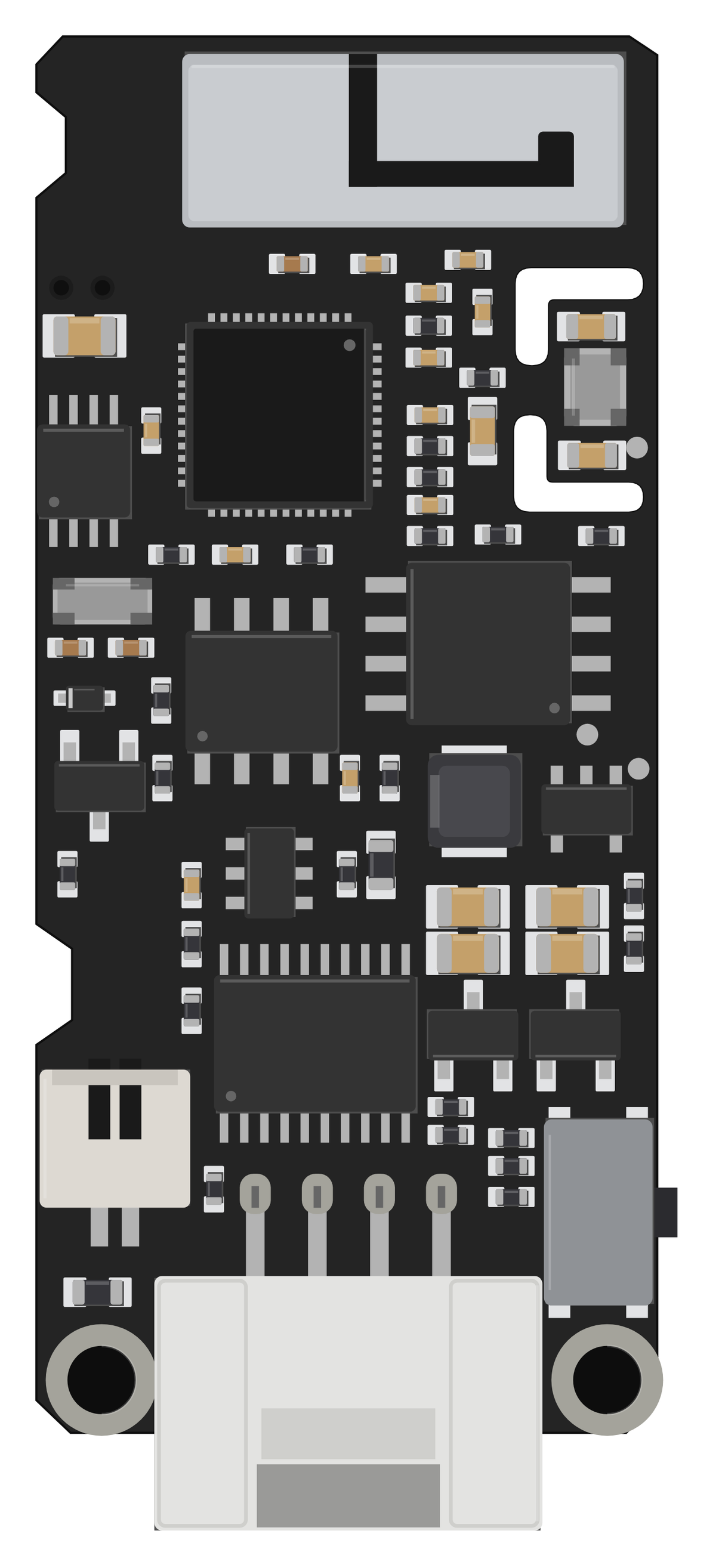
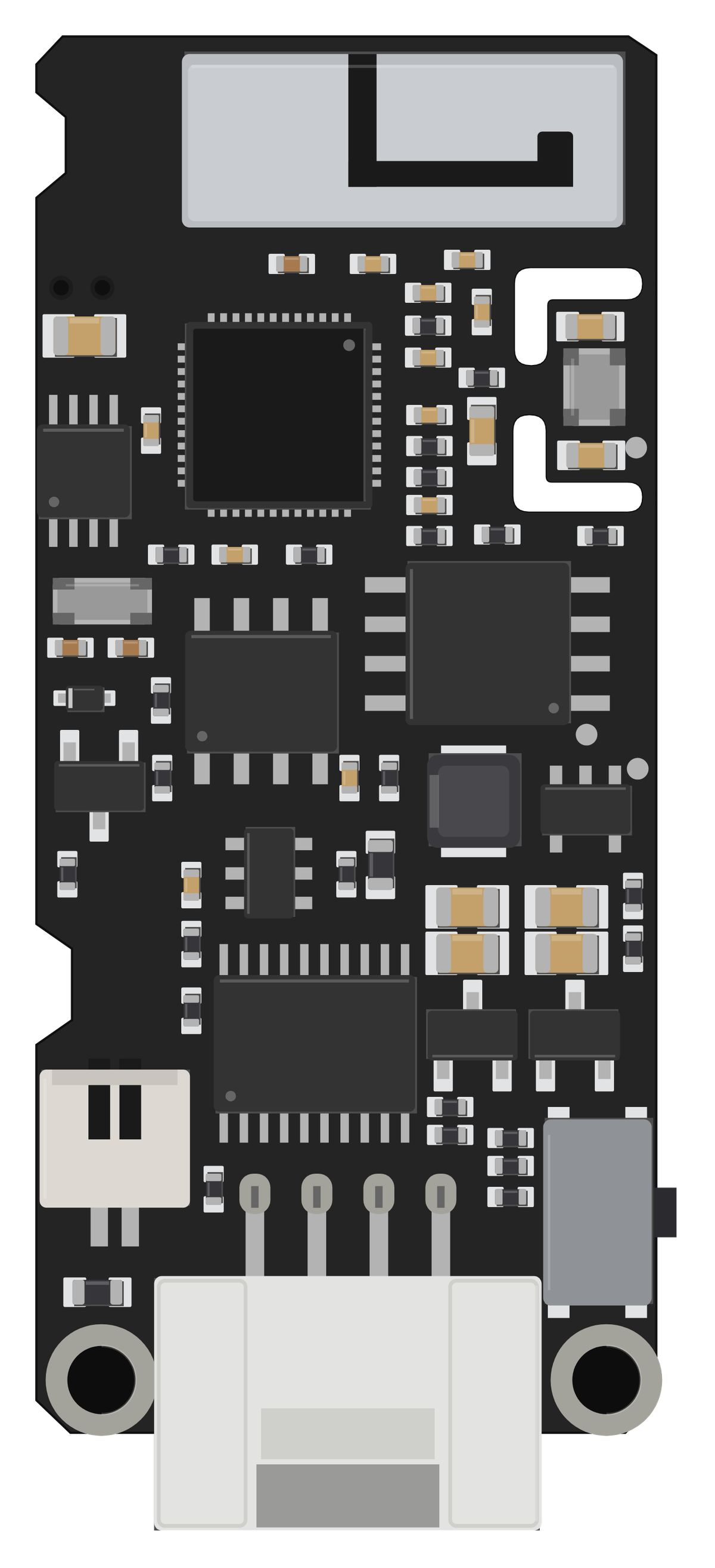
The bare M5Stack-Timer-CAM board drawn to scale at 45 × 20 mm, with no pin labels on it. Made for slide decks, wiring diagrams and project write-ups where a photo is too busy. Take the scalable SVG for print or editing, the high-resolution PNG to drop straight in, or the transparent PNG when you need it with no background behind it.
Pinout diagram
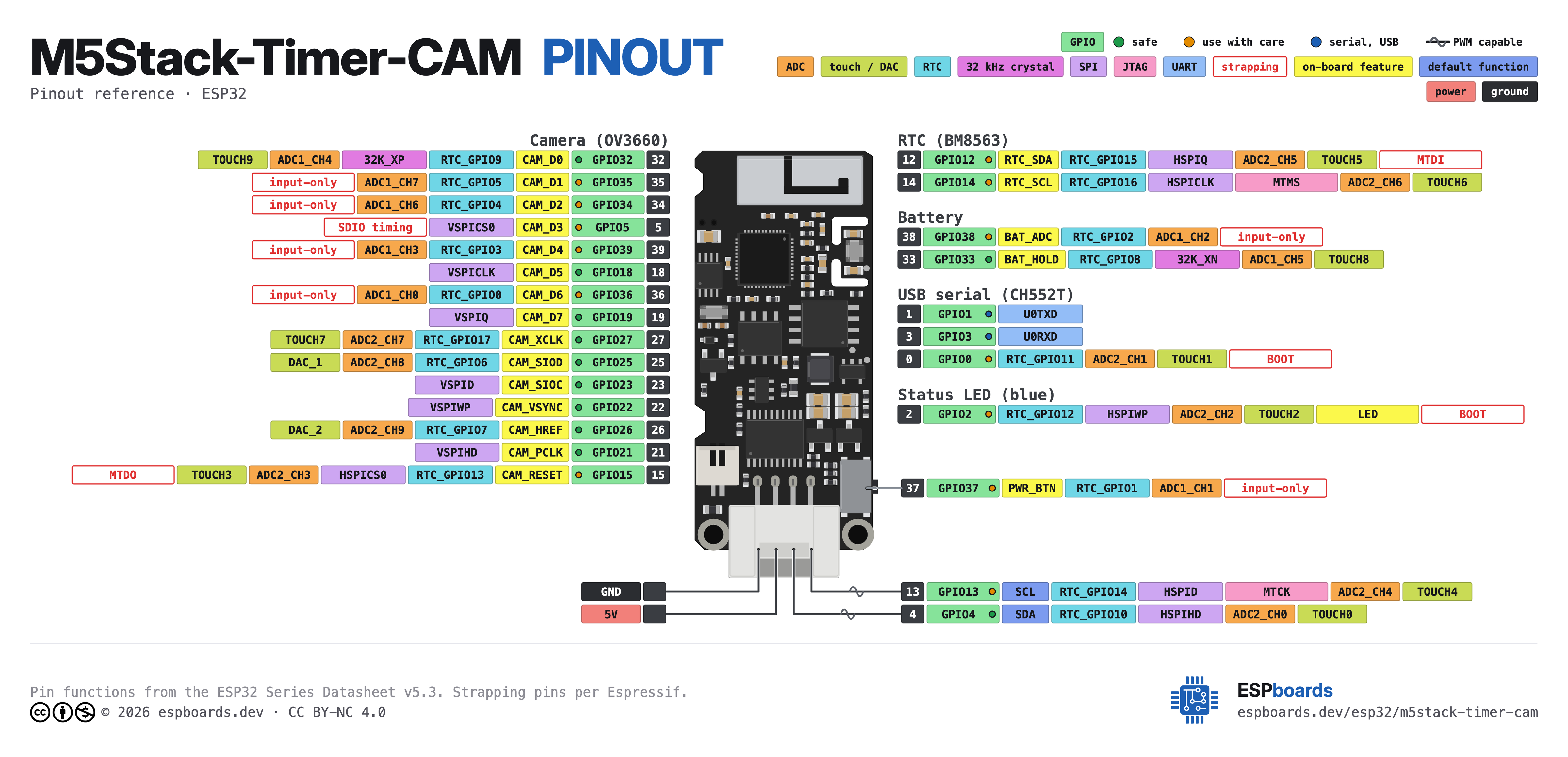
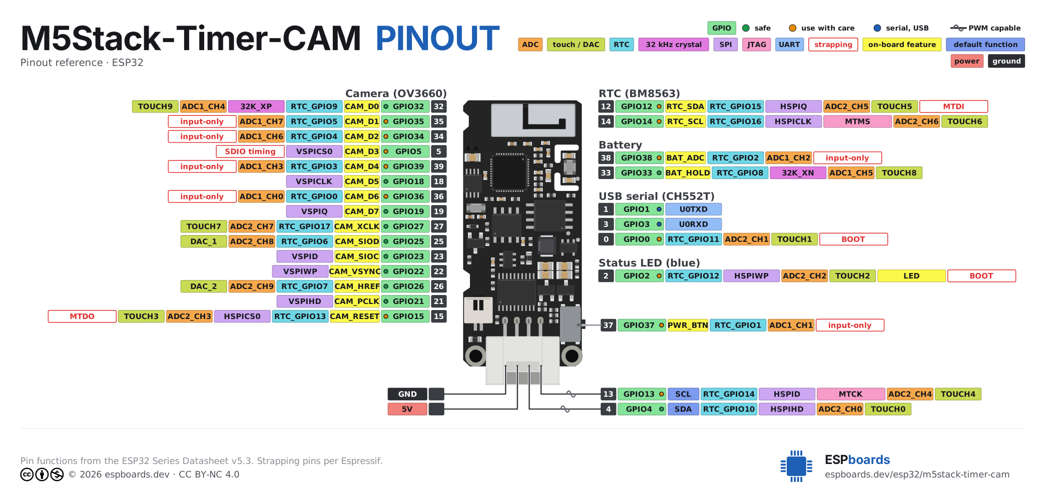
Every pin on both sides of the board with its functions, drawn by ESPboards from the ESP32 Series Datasheet v5.3 - the same sheet shown at the top of this page. The PNG is a high-resolution image for screens, the SVG is vector so it stays sharp at any size, and the PDF is laid out to print on A4 or Letter.
Yours to use, share and adapt for non-commercial work, as long as you credit espboards.dev - the full terms and ready-made credit lines are here.
Specifications
ESP32 · 45 × 20 mm · vs other ESP32 chips →Dimensions

About this board
At its core is the ESP32 - a dual-core Xtensa with both Bluetooth Classic and BLE.
Expect to pay about $15.95 - less than the ~$20 most ESP32 boards go for.
Onboard you'll find 8MB PSRAM, an OV3660 camera (2048x1536), a Grove connector, a BM8563 RTC, battery charging via SH1.0-2P, status LEDs (Status) and Power/Reset buttons.
Where to buy
prices are typical street pricesResources
Similar boards


