
CYD ESP32-1732S019
An ESP32-S3-based development board by CYD, designed for display and user interface applications.

Pinout
24 pins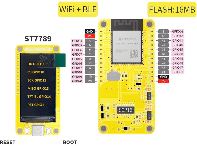
| Pin | GPIO | Labels | Status | Capabilities | Notes |
|---|---|---|---|---|---|
| 1 | 20 | IO20GPIO20 | uart | adc | P1 header pin 1; ESP32-S3 native USB D+ (USB-PWR-DP) |
| 2 | 19 | IO19GPIO19 | uart | adc | P1 header pin 2; ESP32-S3 native USB D- (USB-PWR-DM) |
| 3 | 18 | IO18GPIO18 | safe | adc | P1 header pin 3 |
| 4 | 17 | IO17GPIO17 | safe | adc | P1 header pin 4 |
| 5 | 16 | IO16GPIO16 | safe | adc | P1 header pin 5 |
| 6 | 15 | IO15GPIO15 | safe | adc | P1 header pin 6 |
| 7 | 7 | IO7GPIO7 | safe | adc · touch | P1 header pin 7 |
| 8 | 6 | IO6GPIO6 | safe | adc · touch | P1 header pin 8 |
| 9 | 5 | IO5GPIO5 | safe | adc · touch | P1 header pin 9 |
| 10 | 4 | IO4GPIO4 | safe | adc · touch | P1 header pin 10 |
| 11 | - | 3V33.3V | power | - | P1 header pin 11; 3.3V output |
| 12 | - | GND | ground | - | P1 header pin 12 |
| 13 | - | 5V | power | - | P2 header pin 1; 5V rail (USB VBUS) |
| 14 | - | GND | ground | - | P2 header pin 2 |
| 15 | 21 | IO21GPIO21 | safe | - | P2 header pin 3 |
| 16 | 47 | IO47GPIO47 | strapping | - | P2 header pin 4 |
| 17 | 48 | IO48GPIO48 | strapping | - | P2 header pin 5 |
| 18 | 45 | IO45GPIO45 | strapping | - | P2 header pin 6; strapping pin (VDD_SPI voltage select) |
| 19 | 38 | IO38GPIO38 | safe | - | P2 header pin 7 |
| 20 | 39 | IO39GPIO39 | strapping | - | P2 header pin 8; JTAG MTCK |
| 21 | 40 | IO40GPIO40 | strapping | - | P2 header pin 9; JTAG MTDO |
| 22 | 41 | IO41GPIO41 | strapping | - | P2 header pin 10; JTAG MTDI |
| 23 | 42 | IO42GPIO42 | strapping | - | P2 header pin 11; JTAG MTMS |
| 24 | 2 | IO2GPIO2 | safe | adc · touch | P2 header pin 12 |
Start with these
11 pins with no boot or system involvementFreely assignable - no strapping, flash, USB or JTAG duties. Ideal first picks for buttons, sensors and LEDs.
Fine - with a little care
sampled at boot or shared with debug/serial| Pin | Label | What to know | Role |
|---|---|---|---|
| IO47 | SPICLK_P | Only the 1.8 V octal parts (ESP32-S3R8V, ESP32-S3R16V) run the differential memory clock here, and on those the pin works at 1.8 V instead of 3.3 V. On the common 3.3 V modules it is a normal GPIO - several devkits drive their RGB LED from GPIO48. | Other |
| IO48 | SPICLK_N | Only the 1.8 V octal parts (ESP32-S3R8V, ESP32-S3R16V) run the differential memory clock here, and on those the pin works at 1.8 V instead of 3.3 V. On the common 3.3 V modules it is a normal GPIO - several devkits drive their RGB LED from GPIO48. | Other |
| IO45 | GPIO45 | Determines flash/PSRAM power voltage (3.3 V vs 1.8 V) at boot. Must match hardware configuration; using as GPIO can upset flash supply setting. | Strapping |
| IO39 | MTCK (GPIO39) | Default JTAG TCK - keep it free if you debug over JTAG. It is not a flash or PSRAM line on standard modules: those sit on GPIO26-37. | Other |
| IO40 | MTDO (GPIO40) | Default JTAG TDO output for debugging. Using it as GPIO will interfere with JTAG debugging functionality. | Other |
| IO41 | MTDI (GPIO41) | Default JTAG TDI input for debugging. Should be reserved for JTAG or left unused if JTAG is to remain available. | Other |
| IO42 | MTMS (GPIO42) | Default JTAG TMS signal for debugging. Using this pin for other purposes will disable the JTAG interface (unless JTAG is rerouted to USB). | Other |
Only if you know the tricks
wired to flash or USB - expect a fight| Pin | Label | What to know | Role |
|---|---|---|---|
| IO20 | USB_D+ | By default connected to the on-chip USB Serial/JTAG controller. Using it as general GPIO without reconfiguring IO MUX will interfere with USB functionality. | USB |
| IO19 | USB_D- | By default connected to the on-chip USB Serial/JTAG controller. Using it as general GPIO without reconfiguring IO MUX will interfere with USB functionality. | USB |
Pinout notes Across 24 pins, the CYD ESP32-1732S019 exposes 20 GPIO plus 3V3, GND and 5V for power. Beyond plain digital I/O you get 11 ADC-capable pins for sensors and…
Across 24 pins, the CYD ESP32-1732S019 exposes 20 GPIO plus 3V3, GND and 5V for power.
Beyond plain digital I/O you get 11 ADC-capable pins for sensors and battery monitoring and 5 capacitive-touch inputs.
7 of the exposed pins carry boot-time or system duties on the ESP32-S3 (IO47, IO48, IO45 and 4 more) - check the guidance above before wiring anything to them. IO18, IO17, IO16, IO15 and 7 more are free of any such role - the safest first picks.
Getting started
flash your first firmware in ~2 minutesBoard: ESP32S3 Dev Module Flash Size: 16MB (128Mb) Flash Mode: DIO PSRAM: OPI PSRAM Partition Scheme: 16M Flash (3MB APP/9.9MB FATFS) Upload Speed: 921600
// toggle GPIO18 - wire an LED and resistor to it
void setup() {
  pinMode(18, OUTPUT);
}
void loop() {
  digitalWrite(18, HIGH); delay(500);
  digitalWrite(18, LOW);  delay(500);
}[env:cyd-esp32-1732s019]
platform = espressif32
board = esp32-s3-devkitc-1
framework = arduino
monitor_speed = 115200
upload_speed = 921600
board_build.arduino.memory_type = qio_opi
build_flags = -DBOARD_HAS_PSRAMesp32-s3-devkitc-1 - or type it after board =.esp32:
board: esp32-s3-devkitc-1
variant: esp32s3
framework:
type: esp-idf
psram:
mode: octal
speed: 80MHz
# blink - GPIO18
output:
- platform: gpio
pin: 18
id: led_out
light:
- platform: binary
name: "LED"
output: led_outesp32-s3-devkitc-1 (same ids as PlatformIO).esptool.py --chip esp32s3 --port /dev/ttyACM0 \
--baud 921600 write_flash 0x0 firmware.bin--port = your /dev/tty* (macOS/Linux) or COMx (Windows).Specifications
ESP32-S3 · 65 × 32 mm · vs other ESP32 chips →About this board
Inside sits the ESP32-S3 - a dual-core Xtensa with vector extensions suited to AI workloads. Sibling CYD boards cover the ESP32-C3 and ESP32, so you can change radios or horsepower without changing the footprint.
At $10.49 it's cheaper than most CYD boards, which usually run around $22.
Around the module: 8MB (OPI) PSRAM, an IPS LCD 1.9" 170x320 display, a microSD slot and Reset/Boot buttons.
- A capacitive touch variant (ESP32-1732S019C, GT911) is also available
Where to buy
prices are typical street pricesResources
Similar boards
All Cyd boards →

