
LilyGo T-Display-S3
LilyGo T-Display-S3 is a development board based on the ESP32S3 microcontroller using XTENSA architecture.
This board features a maximum CPU frequency of 240 MHz and 16MB flash memory.
About LilyGo T-Display-S3
🚀 The LilyGo T-Display-S3 is a powerful development board featuring an ESP32-S3 chip with integrated WiFi and Bluetooth 5 capabilities. Equipped with a 1.9-inch LCD (270x320) driven by an ST7789V controller, it provides a vibrant display for embedded applications. ⚡
📡 With WiFi 802.11 b/g/n and Bluetooth 5 (LE), it offers seamless wireless connectivity for IoT projects. Its 8MB PSRAM and 16MB Flash memory ensure ample storage and performance.
💾 Designed with multiple GPIOs, PWM, ADC, I2C, and SPI support, it is suitable for various applications, including sensor interfacing, graphical user interfaces, and wireless communication.
Where to Buy LilyGo T-Display-S3

Starting from
$23 per unit


Prices are subject to change. We earn from qualifying purchases as an Amazon Associate.
Technical Specifications
Complete technical specification details for LilyGo T-Display-S3
Quick Setup
Copy-paste configs for LilyGo T-Display-S3 - auto‑generated from this board's exact hardware specs.
In Arduino IDE 2 select Lilygo T Display S3 from the esp32 by Espressif package. In PlatformIO use board = esp32-s3-devkitm-1. ESP32S3 · 240 MHz · 16MB · DIO.
In Arduino IDE 2, open Boards Manager, search "esp32" by Espressif and install it. Then go to Tools → Board and select "Lilygo T Display S3" for the LilyGo T-Display-S3.
LilyGo T-Display-S3 Pinout Diagram
Complete pin reference for LilyGo T-Display-S3
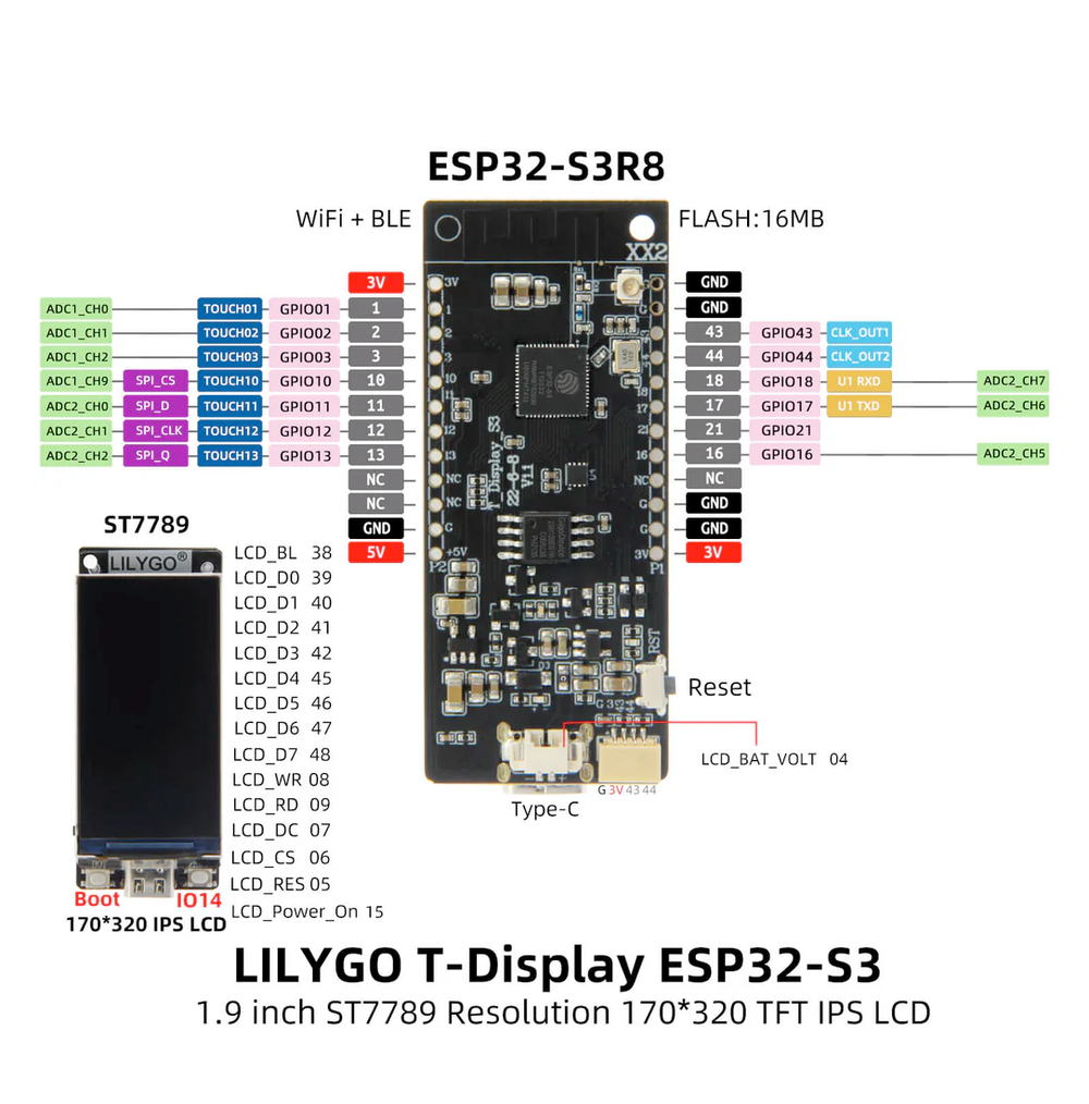
The LilyGo T-Display-S3 pinout provides various digital and analog pins, along with a dedicated display interface. Key pins include:
5V and 3.3V power rails for stable operation.
SDA and SCL for I2C, MISO, MOSI, SCK, and SS for SPI communication.
Additionally, dedicated LCD pins ensure efficient display control.
Safe Pins to Use
These pins are safe for general GPIO usage without boot or system conflicts.
Pins to Avoid or Use with Caution
Reserved for critical functions. Misuse may cause boot failures, programming issues, or system conflicts.
| Pin | Label | Why Avoid | Type |
|---|---|---|---|
| IO3 | GPIO3 | Sampled at reset to select JTAG interface (USB Serial/JTAG controller vs. external pins). Improper use can disable external JTAG or alter debug interface. | 🛠️ Strapping |
| IO10 | FSPICS0 | Used to select the external flash chip. It is required for flash access and cannot be repurposed without losing flash connectivity | ⚡ Flash |
| IO11 | FSPID | Used as a data line for flash (and in-package PSRAM). It should not be used as GPIO when the flash/PSRAM is in use. | ⚡ Flash |
| IO12 | FSPICLK | Drives the flash (and PSRAM) clock. This critical signal must be reserved for memory and not used as general GPIO. | ⚡ Flash |
| IO13 | FSPIQ | Used as a data line for flash/PSRAM transfers. Not available for other uses when flash/PSRAM is connected. | ⚡ Flash |
| IO43 | U0TXD (GPIO43) | Used for bootloader output and UART console logs. If repurposed, you will lose the default serial output (and programming via UART0). | 🪛 Other |
| IO44 | U0RXD (GPIO44) | Used for bootloader input (download mode via serial). If repurposed, you cannot use the default UART0 download mode for programming the chip. | 🪛 Other |
| IO38 | FSPIWP | On flash-equipped chips, this pin is tied to the flash’s WP# (or D3) line. It should be avoided for other use, as it’s needed for flash operations. | ⚡ Flash |
| IO39 | MTCK (GPIO39) | Default JTAG debugging TCK pin. If JTAG is needed, this pin must be free; it may also be used internally for PSRAM chip select on certain modules, so avoid repurposing it. | 🪛 Other |
| IO40 | MTDO (GPIO40) | Default JTAG TDO output for debugging. Using it as GPIO will interfere with JTAG debugging functionality. | 🪛 Other |
| IO41 | MTDI (GPIO41) | Default JTAG TDI input for debugging. Should be reserved for JTAG or left unused if JTAG is to remain available. | 🪛 Other |
| IO42 | MTMS (GPIO42) | Default JTAG TMS signal for debugging. Using this pin for other purposes will disable the JTAG interface (unless JTAG is rerouted to USB). | 🪛 Other |
| IO45 | GPIO45 | Determines flash/PSRAM power voltage (3.3 V vs 1.8 V) at boot. Must match hardware configuration; using as GPIO can upset flash supply setting. | 🛠️ Strapping |
| IO46 | GPIO46 | Must be at a defined level during reset (with GPIO0) to select normal or download boot and UART/USB print mode. This pin is input-only (no output drive), so it should be left for its intended strapping function. | 🛠️ Strapping |
| IO47 | SPICLK_P | Used only on variants with Octal SPI interface (e.g. ESP32-S3R16V) as part of the differential clock pair. On such chips it operates at 1.8 V and is reserved for the high-speed octal SPI clock, not for general GPIO use. | ⚡ Flash |
| IO48 | SPICLK_N | Used only on variants with Octal SPI interface, as the negative leg of the differential clock&. On such chips it operates at 1.8 V; it should be avoided for GPIO to prevent conflicts with the octal flash/PSRAM clock. | ⚡ Flash |
| IO9 | FSPIHD | Connected to external flash (data/hold signal) on most modules. Not recommended for use as GPIO, since it must remain dedicated to flash communication. | ⚡ Flash |
| IO14 | FSPIWP | Connected to external flash (data/write-protect signal). Not recommended as GPIO because it’s reserved for flash operations. | ⚡ Flash |
Useful Links
Datasheets and resources for LilyGo T-Display-S3
LilyGo T-Display-S3 Custom Pin Mapping
Pin configuration and GPIO mapping for LilyGo T-Display-S3
| Pin | Function | ESP Pin | I/O Type | Description |
|---|---|---|---|---|
| 1 | 3V3 | 3.3V | POWER OUTPUT | 3.3V power output |
| 2 | GND | GND | POWER GROUND | Ground connection |
| 3 | 5V | 5V | POWER INPUT | 5V power input for the board |
| 5 | IO1 | IO1 | BIDIRECTIONAL | GPIO, Touch, ADC |
| 6 | IO2 | IO2 | BIDIRECTIONAL | GPIO, Touch, ADC |
| 7 | IO3 | IO3 | BIDIRECTIONAL | GPIO, Touch, ADC |
| 8 | IO10 | SPI_CS | BIDIRECTIONAL | GPIO, SPI Chip Select |
| 9 | IO11 | SPI_D | BIDIRECTIONAL | GPIO, SPI Data |
| 10 | IO12 | SPI_CLK | BIDIRECTIONAL | GPIO, SPI Clock |
| 11 | IO13 | SPI_Q | BIDIRECTIONAL | GPIO, SPI Q |
| 12 | IO16 | ADC2_CH5 | BIDIRECTIONAL | GPIO, ADC |
| 13 | IO17 | U1_TXD | BIDIRECTIONAL | GPIO, UART TX |
| 14 | IO18 | U1_RXD | BIDIRECTIONAL | GPIO, UART RX |
| 15 | IO21 | IO21 | BIDIRECTIONAL | GPIO |
| 16 | IO43 | CLK_OUT1 | OUTPUT | GPIO, Clock Output 1 |
| 17 | IO44 | CLK_OUT2 | OUTPUT | GPIO, Clock Output 2 |
| 18 | IO38 | LCD_BL | OUTPUT | GPIO, LCD BL |
| 19 | IO39 | LCD_D0 | OUTPUT | GPIO, LCD Data 0 |
| 20 | IO40 | LCD_D1 | OUTPUT | GPIO, LCD Data 1 |
| 21 | IO41 | LCD_D2 | OUTPUT | GPIO, LCD Data 2 |
| 22 | IO42 | LCD_D3 | OUTPUT | GPIO, LCD Data 3 |
| 23 | IO45 | LCD_D4 | OUTPUT | GPIO, LCD Data 4 |
| 24 | IO46 | LCD_D5 | OUTPUT | GPIO, LCD Data 5 |
| 25 | IO47 | LCD_D6 | OUTPUT | GPIO, LCD Data 6 |
| 26 | IO48 | LCD_D7 | OUTPUT | GPIO, LCD Data 7 |
| 27 | IO5 | LCD_RES | OUTPUT | GPIO, LCD Reset |
| 28 | IO6 | LCD_CS | OUTPUT | GPIO, LCD Chip Select |
| 29 | IO7 | LCD_DC | OUTPUT | GPIO, LCD Data/Command |
| 30 | IO8 | LCD_WR | OUTPUT | GPIO, LCD Write |
| 31 | IO9 | LCD_RD | OUTPUT | GPIO, LCD Read |
| 32 | IO15 | LCD_POWER_ON | OUTPUT | GPIO, LCD Power Enable |
| 33 | IO4 | LCD_BAT_VOLT | INPUT | GPIO, Battery Voltage Sense |
| 34 | IO14 | BUTTON | INPUT | Button |
Pin Mappings
Complete pinout and GPIO mapping for LilyGo T-Display-S3
| Pin | Analog | Touch | PWM | Other |
|---|---|---|---|---|
| 0 | BUTTON_1 | |||
| 1 | A0 | T1 | PWM | |
| 2 | A1 | T2 | PWM | |
| 3 | A2 | T3 | PWM | |
| 4 | PWM | BAT_VOLT | ||
| 10 | A9 | T10 | PWM | SS |
| 11 | A10 | T11 | PWM | MOSI |
| 12 | A11 | T12 | PWM | SCK |
| 13 | A12 | T13 | PWM | MISO |
| 17 | A16 | PWM | SCL | |
| 18 | A17 | PWM | SDA | |
| 43 | PWM | TX | ||
| 44 | PWM | RX |
Default Tools & Configuration
Build and upload settings for LilyGo T-Display-S3
| Setting | Value |
|---|---|
| Bootloader tool | esptool_py |
| Uploader tool | esptool_py |
| Network uploader tool | esp_ota |
| Bootloader address | 0x0 |
| Flash mode | dio |
| Boot mode | qio |
| PSRAM type | opi |
| Maximum upload size | 3072 KB (3145728 bytes) |
| Maximum data size | 320 KB (327680 bytes) |
The LilyGo T-Display-S3 uses esptool_py for uploads , esp_ota for OTA updates, and esptool_py bootloader at 0x0.
Flash mode: dio | Boot mode: qio | PSRAM: opi
Max sketch size: 3072 KB | Max data size: 320 KB
Similar Boards
Other development boards with ESP32S3 microcontroller

LilyGo T-Embed CC1101
LilyGo T-Embed CC1101 development board is based on esp32s3 microcontroller and uses xtensa architecture.

LilyGo T-Eth Lite
LilyGo T-Eth Lite development board is based on esp32 microcontroller and uses xtensa architecture.

TTGO T-OI PLUS RISC-V ESP32-C3
TTGO T-OI PLUS RISC-V ESP32-C3 development board is based on esp32c3 microcontroller and uses riscv32...