
LilyGo T3S3 V1.0 is a development board based on the ESP32S3 microcontroller using XTENSA architecture.
This board features a maximum CPU frequency of 240 MHz and 16MB flash memory.
About LilyGo T3S3 V1.0
🚀 The LilyGo T3S3 V1.0 is an ESP32-S3-based development board designed for high-performance applications. With integrated WiFi and Bluetooth 5, it offers seamless wireless connectivity for IoT projects. ⚡
📡 Featuring a compact design, the T3S3 V1.0 is equipped with 8MB PSRAM and 16MB Flash, ensuring sufficient storage and processing power for complex tasks.
💾 The board includes multiple GPIOs, ADC, PWM, I2C, and SPI support, making it suitable for a wide range of embedded applications.
Technical Specifications
Complete technical specification details for LilyGo T3S3 V1.0
Display
Connectivity
Microcontroller
✨ Features & Pins
Quick Setup
Copy-paste configs for LilyGo T3S3 V1.0 - auto‑generated from this board's exact hardware specs.
In Arduino IDE 2 select Lilygo T3s3 V1 0 from the esp32 by Espressif package. In PlatformIO use board = esp32-s3-devkitm-1. ESP32S3 · 240 MHz · 16MB · DIO.
In Arduino IDE 2, open Boards Manager, search "esp32" by Espressif and install it. Then go to Tools → Board and select "Lilygo T3s3 V1 0" for the LilyGo T3S3 V1.0.
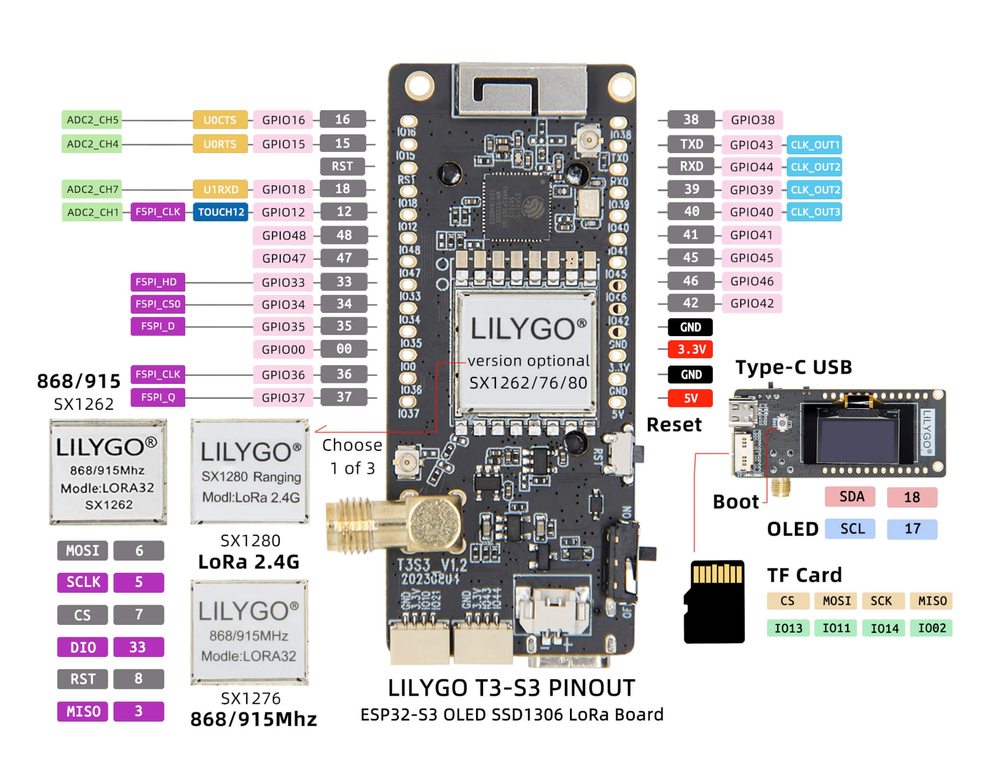
LilyGo T3S3 V1.0 Pinout Diagram
Complete pin reference for LilyGo T3S3 V1.0
Safe Pins to Use
These pins are safe for general GPIO usage without boot or system conflicts
Why Are These Pins Safe?
Pins to Avoid or Use with Caution
Reserved for critical functions. Misuse may cause boot failures, programming issues, or system conflicts.
Boot behavior & flash voltage
Low-level debugging interface
USB Serial/JTAG communication
Memory & PSRAM connections
Debugging & firmware uploads
| PIN | Label | Why Avoid | Type |
|---|---|---|---|
| IO3 | GPIO3 | Sampled at reset to select JTAG interface (USB Serial/JTAG controller vs. external pins). Improper use can disable external JTAG or alter debug interface. | 🛠️ Strapping |
| IO10 | FSPICS0 | Used to select the external flash chip. It is required for flash access and cannot be repurposed without losing flash connectivity | ⚡ Flash |
| IO11 | FSPID | Used as a data line for flash (and in-package PSRAM). It should not be used as GPIO when the flash/PSRAM is in use. | ⚡ Flash |
| IO12 | FSPICLK | Drives the flash (and PSRAM) clock. This critical signal must be reserved for memory and not used as general GPIO. | ⚡ Flash |
| IO13 | FSPIQ | Used as a data line for flash/PSRAM transfers. Not available for other uses when flash/PSRAM is connected. | ⚡ Flash |
| IO19 | USB_D- | By default connected to the on-chip USB Serial/JTAG controller. Using it as general GPIO without reconfiguring IO MUX will interfere with USB functionality. | 🔌 USB |
Useful Links
Datasheets and resources for LilyGo T3S3 V1.0
LilyGo T3S3 V1.0 Custom Pin Mapping
Pin configuration and GPIO mapping for LilyGo T3S3 V1.0
| Pin | Function | ESP Pin | I/O Type | Description |
|---|---|---|---|---|
| 1 | 3V3 | 3.3V | POWER OUTPUT | 3.3V power output |
| 2 | GND | GND | POWER GROUND | Ground connection |
| 3 | 5V | 5V | POWER INPUT | 5V power input |
| 4 | IO1 | GPIO1 | BIDIRECTIONAL | GPIO, ADC, I2C |
| 5 | IO2 | GPIO2 | BIDIRECTIONAL | GPIO, ADC |
| 6 | IO3 | GPIO3 | BIDIRECTIONAL | GPIO, ADC |
| 7 | IO10 | SPI_CS | BIDIRECTIONAL | GPIO, SPI Chip Select |
| 8 | IO11 | SPI_D | BIDIRECTIONAL | GPIO, SPI Data |
| 9 | IO12 | SPI_CLK | BIDIRECTIONAL | GPIO, SPI Clock |
| 10 | IO13 | SPI_Q | BIDIRECTIONAL | GPIO, SPI Q |
| 11 | IO16 | I2C_SCL | BIDIRECTIONAL | GPIO, I2C Clock |
| 12 | IO17 | I2C_SDA | BIDIRECTIONAL | GPIO, I2C Data |
| 13 | IO18 | UART_TX | BIDIRECTIONAL | GPIO, UART TX |
| 14 | IO19 | UART_RX | BIDIRECTIONAL | GPIO, UART RX |
Default Tools & Configuration
Build and upload settings for LilyGo T3S3 V1.0
| Setting | Value |
|---|---|
| Bootloader tool | esptool_py |
| Uploader tool | esptool_py |
| Network uploader tool | esp_ota |
| Bootloader address | 0x0 |
| Flash mode | dio |
| Boot mode | qio |
| PSRAM type | opi |
| Maximum upload size | 3072 KB (3145728 bytes) |
| Maximum data size | 320 KB (327680 bytes) |
The LilyGo T3S3 V1.0 uses esptool_py for uploads , esp_ota for OTA updates, and esptool_py bootloader at 0x0.
Flash mode: dio | Boot mode: qio | PSRAM: opi
Max sketch size: 3072 KB | Max data size: 320 KB
Similar Boards
Other development boards with ESP32S3 microcontroller

LilyGo T-Deck
LilyGo T-Deck development board is based on esp32s3 microcontroller and uses xtensa architecture.

LilyGo T-Display-S3 AMOLED Touch
LilyGo T-Display-S3 AMOLED Touch development board is based on esp32s3 microcontroller and uses undefined...

LilyGo T-Deck Plus
LilyGo T-Deck Plus development board is based on esp32s3 microcontroller and uses xtensa architecture.