
ESP32S3 CAM LCD
An ESP32-S3-based board featuring a 2MP camera and LCD display, ideal for image recognition and audio processing tasks.

ESP32S3 CAM LCD Pinout
35 pins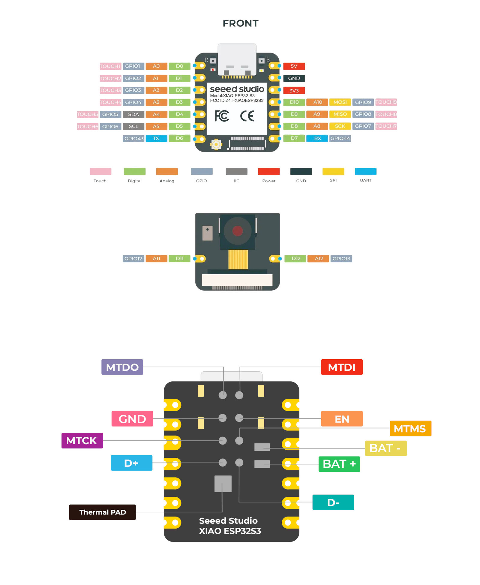
| Pin | GPIO | Labels | Status | Capabilities | Notes |
|---|---|---|---|---|---|
| 1 | 0 | MIC_CLK | strapping | - | |
| 2 | 1 | MIC_DATAPWM | safe | - | |
| 3 | 2 | TFT_DCPWM | safe | - | |
| 4 | 3 | Y5_GPIO_NUMPWM | strapping | - | |
| 5 | 4 | TFT_WRPWM | safe | - | |
| 6 | 5 | TFT_D7PWM | safe | - | |
| 7 | 6 | TFT_D6PWM | safe | - | |
| 8 | 7 | TFT_D5PWM | safe | - | |
| 9 | 8 | TFT_BITSTFT_D4PWM | safe | - | |
| 10 | 9 | SDMMC_CLKPWM | strapping | - | |
| 11 | 10 | SSTFT_D3PWM | strapping | spi | |
| 12 | 11 | MOSIPCLK_GPIO_NUMPWM | strapping | spi | |
| 13 | 12 | SCKY6_GPIO_NUMPWM | strapping | spi | |
| 14 | 13 | MISOY2_GPIO_NUMPWM | strapping | spi | |
| 15 | 14 | Y4_GPIO_NUMPWM | strapping | - | |
| 16 | 15 | TFT_D2PWM | safe | - | |
| 17 | 16 | TFT_D1PWM | safe | - | |
| 18 | 17 | SDAI2C_SDASIOD_GPIO_NUMPWM | safe | i2c | |
| 19 | 18 | SCLI2C_SCLSIOC_GPIO_NUMPWM | safe | i2c | |
| 20 | 19 | SDMMC_DATAPWM | uart | - | |
| 21 | 20 | SDMMC_CMDPWM | uart | - | |
| 22 | 21 | VSYNC_GPIO_NUMPWM | safe | - | |
| 23 | 38 | HREF_GPIO_NUMPWM | safe | - | |
| 24 | 39 | Y9_GPIO_NUMPWM | strapping | - | |
| 25 | 40 | XCLK_GPIO_NUMPWM | strapping | - | |
| 26 | 41 | Y8_GPIO_NUMPWM | strapping | - | |
| 27 | 42 | Y7_GPIO_NUMPWM | strapping | - | |
| 28 | 43 | TXPWM | uart | uart | |
| 29 | 44 | RXPWM | uart | uart | |
| 30 | 45 | TFT_D0PWM | strapping | - | |
| 31 | 47 | Y3_GPIO_NUM | strapping | - | |
| 32 | 320 | TFT_HEIGHT | safe | - | |
| 33 | 480 | TFT_WIDTH | safe | - | |
| 34 | 40000000 | TFT_FREQ | safe | - | |
| 35 | - | PWDN_GPIO_NUMRESET_GPIO_NUM | safe | - |
Start with these
16 pins with no boot or system involvementFreely assignable - no strapping, flash, USB or JTAG duties. Ideal first picks for buttons, sensors and LEDs.
Fine - with a little care
16 pins · 11 things to knowMIC_CLKGPIO0 Bootstrapping pin (Chip boot mode selection) Strapping
Must be pulled high (default) or low (to enter UART download mode) at reset. Using it for other functions can interfere with boot mode configuration.
Y5_GPIO_NUMGPIO3 Bootstrapping pin (controls JTAG signal source) Strapping
Sampled at reset to select JTAG interface (USB Serial/JTAG controller vs. external pins). Improper use can disable external JTAG or alter debug interface.
SDMMC_CLKGPIO9SSGPIO10MOSIGPIO11SCKGPIO12MISOGPIO13Y4_GPIO_NUMGPIO14 General-purpose SPI2 (FSPI) IO MUX pins Other
IO MUX pin of the general-purpose SPI2 (FSPI) bus, not of the in-package flash - that sits on GPIO26-32. The datasheet lists it as a priority-2 pin ("can be freely used without restrictions"), so it is only taken if your board wires flash, an SD card or a display to FSPI.
- SDMMC_CLKGeneral-purpose SPI2 (FSPI) IO MUX pin - hold/data line (FSPIHD)
- SSGeneral-purpose SPI2 (FSPI) IO MUX pin - chip select (FSPICS0)
- MOSIGeneral-purpose SPI2 (FSPI) IO MUX pin - data in (FSPID)
- SCKGeneral-purpose SPI2 (FSPI) IO MUX pin - clock (FSPICLK)
- MISOGeneral-purpose SPI2 (FSPI) IO MUX pin - data out (FSPIQ)
- Y4_GPIO_NUMGeneral-purpose SPI2 (FSPI) IO MUX pin - write-protect/data line (FSPIWP)
Y9_GPIO_NUMGPIO39 JTAG test clock (MTCK); IO MUX alternates CLK_OUT3 and SUBSPICS1 (chip select on the alternative SUBSPI memory bus, unused on standard modules) JTAG
Default JTAG TCK - keep it free if you debug over JTAG. It is not a flash or PSRAM line on standard modules: those sit on GPIO26-37.
XCLK_GPIO_NUMGPIO40 JTAG test data out pin (MTDO) JTAG
Default JTAG TDO output for debugging. Using it as GPIO will interfere with JTAG debugging functionality.
Y8_GPIO_NUMGPIO41 JTAG test data in pin (MTDI) JTAG
Default JTAG TDI input for debugging. Should be reserved for JTAG or left unused if JTAG is to remain available.
Y7_GPIO_NUMGPIO42 JTAG test mode select pin (MTMS) JTAG
Default JTAG TMS signal for debugging. Using this pin for other purposes will disable the JTAG interface (unless JTAG is rerouted to USB).
TXGPIO43 UART0 transmit pin (U0TXD), default serial console TX UART
Used for bootloader output and UART console logs. If repurposed, you will lose the default serial output (and programming via UART0).
RXGPIO44 UART0 receive pin (U0RXD), default serial console RX UART
Used for bootloader input (download mode via serial). If repurposed, you cannot use the default UART0 download mode for programming the chip.
TFT_D0GPIO45 Bootstrapping pin (selects VDD_SPI flash voltage) Strapping
Determines flash/PSRAM power voltage (3.3 V vs 1.8 V) at boot. Must match hardware configuration; using as GPIO can upset flash supply setting.
Y3_GPIO_NUMGPIO47 Octal SPI differential clock positive leg (SPICLK_P_DIFF), used only by the 1.8 V octal flash/PSRAM variants Other
Only the 1.8 V octal parts (ESP32-S3R8V, ESP32-S3R16V) run the differential memory clock here, and on those the pin works at 1.8 V instead of 3.3 V. On the common 3.3 V modules it is a normal GPIO - several devkits drive their RGB LED from GPIO48.
Only if you know the tricks
2 pins · 1 thing to knowSDMMC_DATAGPIO19SDMMC_CMDGPIO20 USB OTG differential data pair (D- and D+) USB
By default connected to the on-chip USB Serial/JTAG controller. Using it as general GPIO without reconfiguring IO MUX will interfere with USB functionality.
- SDMMC_DATAUSB OTG negative differential data line (USB_D-)
- SDMMC_CMDUSB OTG positive differential data line (USB_D+)
The ESP32S3 CAM LCD breaks out 35 pins in total: 34 GPIO for your project.
Peripheral wiring is straightforward: I²C is mapped to SDA on GPIO17 and SCL on GPIO18; the SPI bus (MOSI, MISO, SCK, SS) is broken out in full; TX/RX on GPIO43 and GPIO44 cover serial logging and flashing.
16 of the exposed pins carry boot-time or system duties on the ESP32-S3 (MIC_CLK, Y5_GPIO_NUM, SDMMC_CLK and 13 more) - check the guidance above before wiring anything to them. MIC_DATA, TFT_DC, TFT_WR, TFT_D7 and 12 more are free of any such role - the safest first picks.
Getting started
flash your first firmware in ~2 minutesBoard: ESP32S3 Dev Module USB CDC On Boot: Enabled Flash Size: 16MB (128Mb) Flash Mode: DOUT PSRAM: OPI PSRAM Partition Scheme: 16M Flash (3MB APP/9.9MB FATFS) Upload Speed: 921600
// toggle GPIO1 - wire an LED and resistor to it
void setup() {
  pinMode(1, OUTPUT);
}
void loop() {
  digitalWrite(1, HIGH); delay(500);
  digitalWrite(1, LOW);  delay(500);
}[env:esp32s3camlcd]
platform = espressif32
board = esp32-s3-devkitc-1
framework = arduino
monitor_speed = 115200
upload_speed = 921600
board_build.arduino.memory_type = qio_opi
build_flags = -DBOARD_HAS_PSRAMesp32-s3-devkitc-1 - or type it after board =.esp32:
board: esp32-s3-devkitc-1
variant: esp32s3
framework:
type: esp-idf
psram:
mode: octal
speed: 80MHz
# blink - GPIO1
output:
- platform: gpio
pin: 1
id: led_out
light:
- platform: binary
name: "LED"
output: led_outesp32-s3-devkitc-1 (same ids as PlatformIO).esptool.py --chip esp32s3 --port /dev/ttyACM0 \
--baud 921600 write_flash 0x0 firmware.bin--port = your /dev/tty* (macOS/Linux) or COMx (Windows).Specifications
ESP32-S3 · vs other ESP32 chips →About this board
Inside sits the ESP32-S3 - a dual-core Xtensa with vector extensions suited to AI workloads.
With 34 GPIO broken out, you get more pins to play with than most ESP32-S3 boards offer.
Around the module: 8MB (OPI) PSRAM, an LCD display, an OV2640 camera (1600x1200), a microSD slot and a microphone.
- ESP32-S3-WROOM-1 N16R8 (16MB flash + 8MB octal PSRAM)
- 18-pin SPI/QSPI screen interface (LCD connector); some units ship with dual USB-C ports
Where to buy
prices are typical street pricesResources
Similar boards

